SLVSE31C January 2018 – July 2018 TPSM84209
PRODUCTION DATA.
- 1 Features
- 2 Applications
- 3 Description
- 4 Revision History
- 5 Pin Configuration and Functions
- 6 Specifications
-
7 Detailed Description
- 7.1 Overview
- 7.2 Functional Block Diagram
- 7.3
Feature Description
- 7.3.1 Adjusting the Output Voltage
- 7.3.2 Input Capacitor Selection
- 7.3.3 Undervoltage Lockout (UVLO)
- 7.3.4 Output Capacitor Selection
- 7.3.5 Feed-Forward Capacitor
- 7.3.6 Operating Range
- 7.3.7 Output Current Rating
- 7.3.8 Enable (EN)
- 7.3.9 Internal Soft Start
- 7.3.10 Safe Start-Up Into Prebiased Outputs
- 7.3.11 Light Load Efficiency / Eco-Mode
- 7.3.12 Voltage Dropout
- 7.3.13 Overcurrent Protection
- 7.3.14 Output Overvoltage Protection (OVP)
- 7.3.15 Thermal Performance
- 7.3.16 Thermal Shutdown
- 7.4 Device Functional Modes
- 8 Application and Implementation
- 9 Power Supply Recommendations
- 10Layout
- 11Device and Documentation Support
- 12Mechanical, Packaging, and Orderable Information
Package Options
Refer to the PDF data sheet for device specific package drawings
Mechanical Data (Package|Pins)
- RKH|9
Thermal pad, mechanical data (Package|Pins)
Orderable Information
7.3.1 Adjusting the Output Voltage
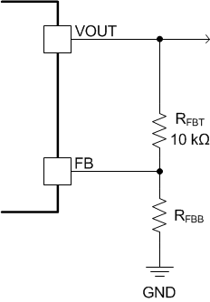
A resistor divider connected to the FB pin (pin 1) programs the output voltage of the TPSM84209. The output voltage adjustment range is from 1.2 V to 6 V. Figure 17 shows the feedback resistor connection for setting the output voltage. The recommended value of RFBT is 10 kΩ. Table 1 lists the closest standard E96 value for the RFBB resistor for a number of common output voltages. For other output voltages, the value of the required RFFB resistor can be calculated using Equation 1.
Equation 1. 

 Figure 17. Setting the Output Voltage
 Table 1. Standard RFBB Resistor Values
| VOUT (V) | RFBB (kΩ) | VOUT (V) | RFBB (kΩ) | |
|---|---|---|---|---|
| 1.2 | 10.0 | 3.7 | 1.96 | |
| 1.3 | 8.45 | 3.8 | 1.87 | |
| 1.4 | 7.50 | 3.9 | 1.82 | |
| 1.5 | 6.65 | 4.0 | 1.74 | |
| 1.6 | 6.04 | 4.1 | 1.69 | |
| 1.7 | 5.36 | 4.2 | 1.65 | |
| 1.8 | 4.99 | 4.3 | 1.62 | |
| 1.9 | 4.64 | 4.4 | 1.58 | |
| 2.0 | 4.22 | 4.5 | 1.54 | |
| 2.1 | 4.02 | 4.6 | 1.50 | |
| 2.2 | 3.74 | 4.7 | 1.47 | |
| 2.3 | 3.48 | 4.8 | 1.43 | |
| 2.4 | 3.32 | 4.9 | 1.40 | |
| 2.5 | 3.16 | 5.0 | 1.37 | |
| 2.6 | 3.01 | 5.1 | 1.33 | |
| 2.7 | 2.87 | 5.2 | 1.30 | |
| 2.8 | 2.74 | 5.3 | 1.27 | |
| 2.9 | 2.61 | 5.4 | 1.24 | |
| 3.0 | 2.49 | 5.5 | 1.22 | |
| 3.1 | 2.37 | 5.6 | 1.20 | |
| 3.2 | 2.32 | 5.7 | 1.18 | |
| 3.3 | 2.21 | 5.8 | 1.15 | |
| 3.4 | 2.15 | 5.9 | 1.13 | |
| 3.5 | 2.05 | 6.0 | 1.10 | |
| 3.6 | 2.00 |