SLVSE31C January   2018  – July 2018 TPSM84209

PRODUCTION DATA.  

  1. Features
  2. Applications
  3. Description
    1.     Device Images
      1.      Simplified Application
      2.      Efficiency vs Output Current
  4. Revision History
  5. Pin Configuration and Functions
    1.     Pin Functions
  6. Specifications
    1. 6.1 Absolute Maximum Ratings
    2. 6.2 ESD Ratings
    3. 6.3 Recommended Operating Conditions
    4. 6.4 Thermal Information
    5. 6.5 Electrical Characteristics
    6. 6.6 Typical Characteristics (VIN = 5 V)
    7. 6.7 Typical Characteristics (VIN = 12 V)
    8. 6.8 Typical Characteristics (VIN = 24 V)
  7. Detailed Description
    1. 7.1 Overview
    2. 7.2 Functional Block Diagram
    3. 7.3 Feature Description
      1. 7.3.1  Adjusting the Output Voltage
      2. 7.3.2  Input Capacitor Selection
      3. 7.3.3  Undervoltage Lockout (UVLO)
      4. 7.3.4  Output Capacitor Selection
      5. 7.3.5  Feed-Forward Capacitor
      6. 7.3.6  Operating Range
      7. 7.3.7  Output Current Rating
      8. 7.3.8  Enable (EN)
      9. 7.3.9  Internal Soft Start
      10. 7.3.10 Safe Start-Up Into Prebiased Outputs
      11. 7.3.11 Light Load Efficiency / Eco-Mode
      12. 7.3.12 Voltage Dropout
      13. 7.3.13 Overcurrent Protection
      14. 7.3.14 Output Overvoltage Protection (OVP)
      15. 7.3.15 Thermal Performance
      16. 7.3.16 Thermal Shutdown
    4. 7.4 Device Functional Modes
      1. 7.4.1 Active Mode
      2. 7.4.2 Eco-Mode Operation
      3. 7.4.3 Shutdown Mode
  8. Application and Implementation
    1. 8.1 Application Information
    2. 8.2 Typical Application
      1. 8.2.1 Design Requirements
      2. 8.2.2 Detailed Design Procedure
        1. 8.2.2.1 Custom Design With WEBENCH® Tools
        2. 8.2.2.2 Output Voltage Setpoint
        3. 8.2.2.3 Input Capacitors
        4. 8.2.2.4 Output Capacitors
        5. 8.2.2.5 Enable Control
      3. 8.2.3 Application Waveforms
  9. Power Supply Recommendations
  10. 10Layout
    1. 10.1 Layout Guidelines
    2. 10.2 Layout Examples
    3. 10.3 EMI
      1. 10.3.1 EMI Plots
    4. 10.4 Package Specifications
  11. 11Device and Documentation Support
    1. 11.1 Device Support
      1. 11.1.1 Third-Party Products Disclaimer
    2. 11.2 Custom Design With WEBENCH® Tools
    3. 11.3 Receiving Notification of Documentation Updates
    4. 11.4 Community Resources
    5. 11.5 Trademarks
    6. 11.6 Electrostatic Discharge Caution
    7. 11.7 Glossary
  12. 12Mechanical, Packaging, and Orderable Information
    1. 12.1 Tape and Reel Information

Package Options

Refer to the PDF data sheet for device specific package drawings

Mechanical Data (Package|Pins)
  • RKH|9
Thermal pad, mechanical data (Package|Pins)
Orderable Information

Typical Characteristics (VIN = 24 V)

TA = 25°C, unless otherwise noted.
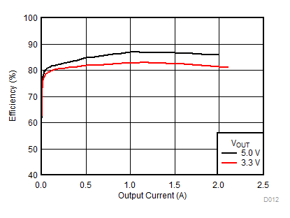
TPSM84209 D012_24Veff3.gif
Figure 12. Efficiency vs Output Current
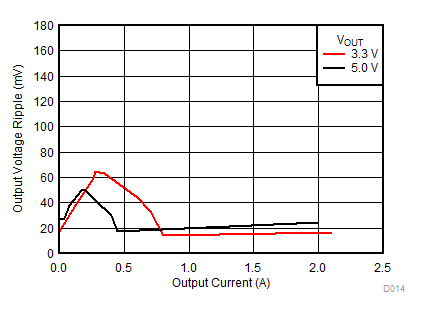
TPSM84209 D014_24VRippleC.gif
COUT = 2× 47 µF ceramic
Figure 14. Voltage Ripple vs Output Current
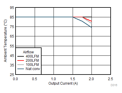
TPSM84209 D016_24to5V85.gif
VOUT = 5 V
Figure 16. Safe Operating Area
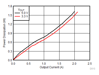
TPSM84209 D013_24VPdisB.gif
Figure 13. Power Dissipation vs Output Current
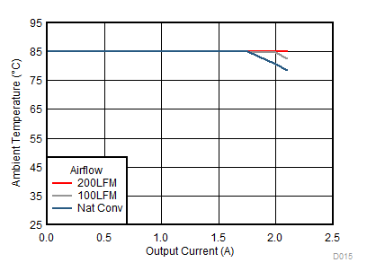
TPSM84209 D015_24to33V85.gif
VOUT = 3.3 V
Figure 15. Safe Operating Area