SLVSE31C January 2018 – July 2018 TPSM84209
PRODUCTION DATA.
- 1 Features
- 2 Applications
- 3 Description
- 4 Revision History
- 5 Pin Configuration and Functions
- 6 Specifications
-
7 Detailed Description
- 7.1 Overview
- 7.2 Functional Block Diagram
- 7.3
Feature Description
- 7.3.1 Adjusting the Output Voltage
- 7.3.2 Input Capacitor Selection
- 7.3.3 Undervoltage Lockout (UVLO)
- 7.3.4 Output Capacitor Selection
- 7.3.5 Feed-Forward Capacitor
- 7.3.6 Operating Range
- 7.3.7 Output Current Rating
- 7.3.8 Enable (EN)
- 7.3.9 Internal Soft Start
- 7.3.10 Safe Start-Up Into Prebiased Outputs
- 7.3.11 Light Load Efficiency / Eco-Mode
- 7.3.12 Voltage Dropout
- 7.3.13 Overcurrent Protection
- 7.3.14 Output Overvoltage Protection (OVP)
- 7.3.15 Thermal Performance
- 7.3.16 Thermal Shutdown
- 7.4 Device Functional Modes
- 8 Application and Implementation
- 9 Power Supply Recommendations
- 10Layout
- 11Device and Documentation Support
- 12Mechanical, Packaging, and Orderable Information
Package Options
Refer to the PDF data sheet for device specific package drawings
Mechanical Data (Package|Pins)
- RKH|9
Thermal pad, mechanical data (Package|Pins)
Orderable Information
7.3.11 Light Load Efficiency / Eco-Mode
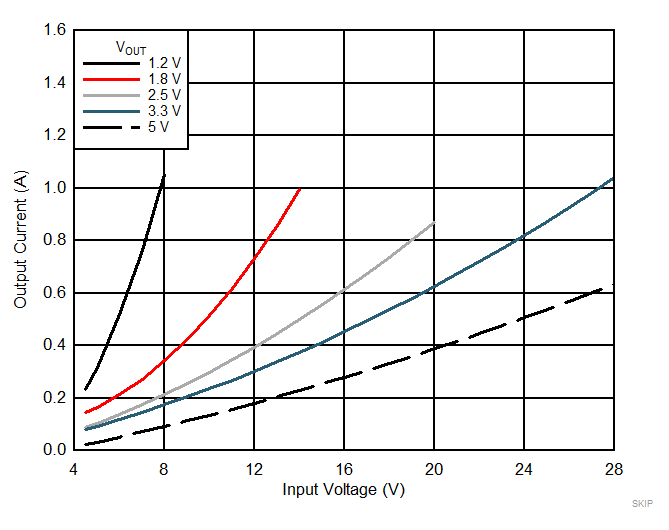
The TPSM84209 device is designed to operate in high-efficiency, pulse-skipping mode under light load conditions. As the load current on the output is decreased, a point is reached where the energy delivered by a single switching pulse is more than the load can absorb. This causes the output voltage to rise slightly. This rise in output voltage is sensed by the feedback loop, and the device responds by skipping one or more switching cycles until the output voltages falls back to the setpoint. At very light loads or no load, many switching cycles are skipped. The observed effect during this pulse-skipping mode of operation is an increase in the peak-to-peak ripple voltage and a decrease in the ripple frequency. The load current where pulse skipping begins is a function of the input voltage and output voltage. Figure 26 is a plot of the pulse-skipping threshold current as a function of input voltage for a number of popular output voltages.
 Figure 26. Pulse-Skipping Threshold