SLVSDF8B December 2016 – July 2017 TPSM84A22
PRODUCTION DATA.
- 1 Features
- 2 Applications
- 3 Description
- 4 Revision History
- 5 Pin Configuration and Functions
- 6 Specifications
-
7 Detailed Description
- 7.1 Overview
- 7.2 Functional Block Diagram
- 7.3
Feature Description
- 7.3.1 Adjusting the Output Voltage (VADJ)
- 7.3.2 Input and Output Capacitance
- 7.3.3 Transient Response
- 7.3.4 Oscillator Frequency
- 7.3.5 External Clock Syncronization
- 7.3.6 Soft Start
- 7.3.7 Power Good (PGOOD)
- 7.3.8 Gate Driver (VG)
- 7.3.9 Startup into Pre-biased Outputs
- 7.3.10 Thermal Shutdown
- 7.3.11 Overcurrent Protection
- 7.3.12 Output Undervoltage/Overvoltage Protection
- 7.3.13 Enable (EN)
- 7.3.14 Undervoltage Lockout (UVLO)
- 7.4 Device Functional Modes
- 8 Application and Implementation
- 9 Power Supply Recommendations
- 10Layout
- 11Device and Documentation Support
- 12Mechanical, Packaging, and Orderable Information
Package Options
Mechanical Data (Package|Pins)
- MOJ|20
Thermal pad, mechanical data (Package|Pins)
Orderable Information
7.3.13 Enable (EN)
The EN pin provides electrical on and off control of the TPSM84A22. Once the EN pin voltage exceeds the threshold voltage, the device starts operation. If the EN pin voltage is pulled below the threshold voltage, the module stops switching and enters a low power state. There is no voltage hysteresis in the EN threshold. The rising and falling voltage thresholds occur at the same level. The EN pin has an internal pull-up current source, allowing the user to float the EN pin for enabling the device.
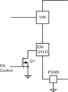
If an application requires controlling the EN pin, use an open drain/collector device or a suitable logic gate to interface with the pin. Figure 16 shows controlling the EN/UVLO pin using a MOSFET, Q1. Turning Q1 on, disables the device. Using a voltage superviser to control the EN pin allows control of the turn-on and turn-off of the device as opposed to relying on the ramp up or down of the input voltage source.
 Figure 16. Enable Control