SLVSDF8B December 2016 – July 2017 TPSM84A22
PRODUCTION DATA.
- 1 Features
- 2 Applications
- 3 Description
- 4 Revision History
- 5 Pin Configuration and Functions
- 6 Specifications
-
7 Detailed Description
- 7.1 Overview
- 7.2 Functional Block Diagram
- 7.3
Feature Description
- 7.3.1 Adjusting the Output Voltage (VADJ)
- 7.3.2 Input and Output Capacitance
- 7.3.3 Transient Response
- 7.3.4 Oscillator Frequency
- 7.3.5 External Clock Syncronization
- 7.3.6 Soft Start
- 7.3.7 Power Good (PGOOD)
- 7.3.8 Gate Driver (VG)
- 7.3.9 Startup into Pre-biased Outputs
- 7.3.10 Thermal Shutdown
- 7.3.11 Overcurrent Protection
- 7.3.12 Output Undervoltage/Overvoltage Protection
- 7.3.13 Enable (EN)
- 7.3.14 Undervoltage Lockout (UVLO)
- 7.4 Device Functional Modes
- 8 Application and Implementation
- 9 Power Supply Recommendations
- 10Layout
- 11Device and Documentation Support
- 12Mechanical, Packaging, and Orderable Information
Package Options
Mechanical Data (Package|Pins)
- MOJ|20
Thermal pad, mechanical data (Package|Pins)
Orderable Information
10.2 Layout Examples
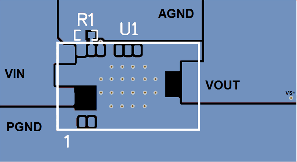
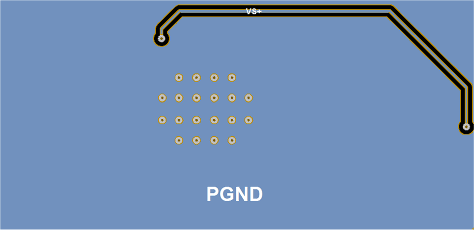
The layout shown in Figure 21 shows the minimum solution size with only a single voltage setting resistor (R1) as the only additional required component. Figure 22 shows a typical internal PCB layer with a trace connecting the VS+ pin to VOUT near the load.
 Figure 21. Minimum Component Layout
  Figure 22. VS+ Trace on Internal Layer
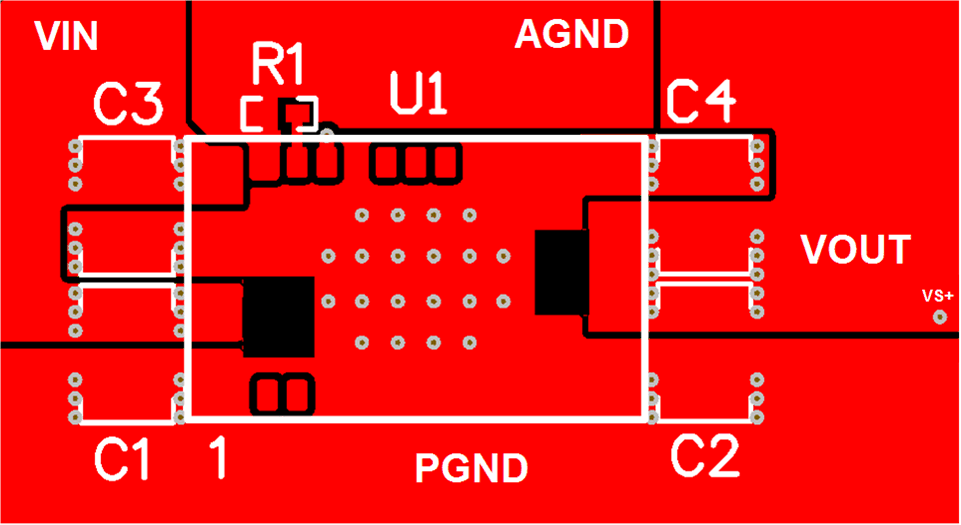
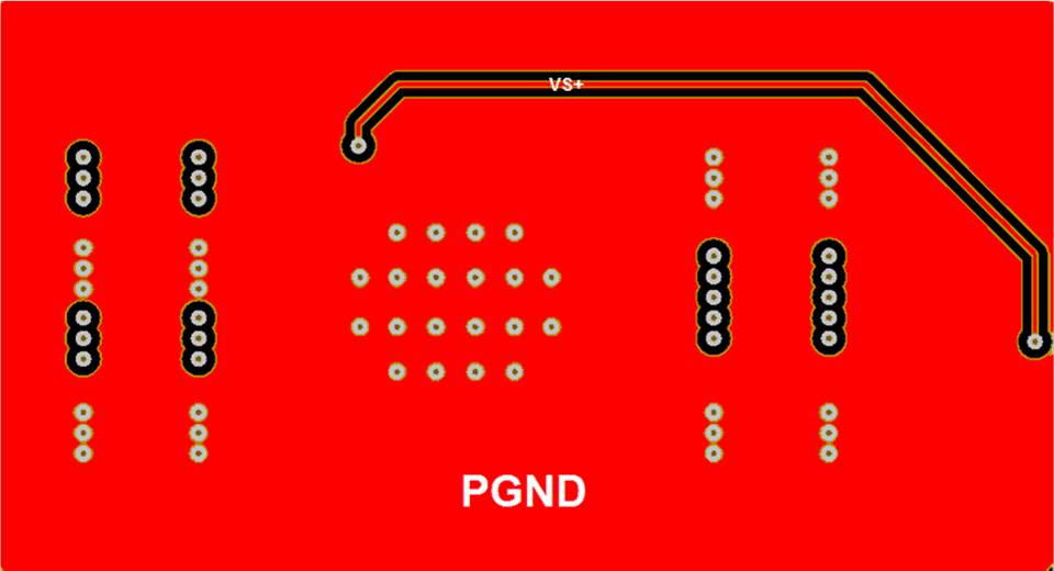
 Figure 23 shows a layout with the placement of additional ceramic input capacitors (C1, C3) and ceramic output capacitors (C2, C4) for designs that require additional ripple reduction or improved transient response. Figure 24 shows a typical internal PCB layer with a trace connecting the VS+ pin to VOUT near the load.
 Figure 23. Layout with Optional CIN and COUT
  Figure 24. VS+ Trace on Internal Layer