SLWS181K October 2005 – December 2015 TRF3761-A , TRF3761-B , TRF3761-C , TRF3761-E , TRF3761-F , TRF3761-G , TRF3761-H , TRF3761-J
PRODUCTION DATA.
- 1 Features
- 2 Applications
- 3 Description
- 4 Revision History
- 5 Device Comparison Table
- 6 Pin Configuration and Functions
-
7 Specifications
- 7.1 Absolute Maximum Ratings
- 7.2 Recommended Operating Conditions
- 7.3 Thermal Information
- 7.4 Electrical Characteristics
- 7.5 Electrical Characteristics, TRF3761-A
- 7.6 Electrical Characteristics,TRF3761-B
- 7.7 Electrical Characteristics, TRF3761-C
- 7.8 Electrical Characteristics, TRF3761-D
- 7.9 Electrical Characteristics, TRF3761-E
- 7.10 Electrical Characteristics, TRF3761-F
- 7.11 Electrical Characteristics, TRF3761-G
- 7.12 Electrical Characteristics, TRF3761-H
- 7.13 Electrical Characteristics, TRF3761-J
- 7.14 Timing Requirements
- 7.15
Typical Characteristics
- 7.15.1 Typical Characteristics, TRF3761-A (See )
- 7.15.2 Typical Characteristics, TRF3761-B (See )
- 7.15.3 Typical Characteristics, TRF3761-C (See )
- 7.15.4 Typical Characteristics, TRF3761-D (See )
- 7.15.5 Typical Characteristics, TRF3761-E (See )
- 7.15.6 Typical Characteristics, TRF3761-F (See )
- 7.15.7 Typical Characteristics, TRF3761-G (See )
- 7.15.8 Typical Characteristics, TRF3761-H (See )
- 7.15.9 Typical Characteristics, TRF3761-J (See )
-
8 Detailed Description
- 8.1 Overview
- 8.2 Functional Block Diagram
- 8.3 Feature Description
- 8.4 Device Functional Modes
- 8.5 Programming
- 8.6 Register Maps
- 9 Application and Implementation
- 10Power Supply Recommendations
- 11Layout
- 12Device and Documentation Support
- 13Mechanical, Packaging, and Orderable Information
Package Options
Mechanical Data (Package|Pins)
- RHA|40
Thermal pad, mechanical data (Package|Pins)
- RHA|40
Orderable Information
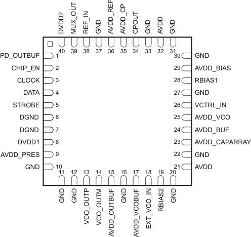
6 Pin Configuration and Functions
RHA Package
40-Pin VQFN
Top View

Pin Functions
| PIN(1) | I/O | DESCRIPTION | |
|---|---|---|---|
| NAME | NO. | ||
| PD_OUTBUF | 1 | I | Once configured in register 1, this pin will control the output buffer. Logic level 0 turns on the buffer and logic level 1 turns off the buffer. |
| CHIP_EN | 2 | I | This pin requires 4.5 to 5.25 V applied for normal operation. Grounding this pin will disable the chip. |
| CLOCK | 3 | I | Serial-programming-interface clock |
| DATA | 4 | I/O | Serial-programming-interface data, used for programming the frequency and other features. |
| STROBE | 5 | I | Serial-programming-interface strobe required to write the data to the chip |
| DGND | 6, 7 | Digital ground | |
| DVDD1 | 8 | Digital power supply, requires 4.5 to 5.25 V, Suggested decoupling, 0.1µF and 10pF capacitors in parallel. | |
| AVDD_PRES | 9 | Power supply for prescaler circuit, requires 4.5 to 5.25 V, Suggested decoupling, 0.1uF and 10pF capacitors in parallel. | |
| VCO_OUTP | 13 | O | VCO output, can be used single ended matched to 50 ohms or in conjuction with VCO_OUTM (pin 14) with a balun. |
| VCO_OUTM | 14 | O | VCO output, can be used single ended matched to 50 ohms or in conjunction with VCO_OUTP (pin 13) with a balun. |
| AVDD_OUTBUF | 15 | Power supply for output buffers, requires 4.5 to 5.25 V, Suggested decoupling, 0.1μF and 10pF capacitors in parallel. | |
| AVDD_VCOBUF | 17 | Power supply for VCO buffers, requires 4.5 to 5.25 V, Suggested decoupling, 0.1μF and 10pF capacitors in parallel. | |
| EXT_VCO_IN | 18 | I | External VCO input to prescaler, If using an external VCO instead of the internal VCO. |
| RBIAS2 | 19 | I/O | External bias resistor for setting the internal reference current requires a 4.75K ohm resister to ground. |
| AVDD | 21 | Analog power supply, requires 4.5 to 5.25 V, Suggested decoupling, 0.1uF and 10μF capacitors in parallel. | |
| AVDD_CAPARRAY | 23 | Power supply for VCO core and buffer, requires 4.5 to 5.25 V, Suggested decoupling, 0.1μF and 10pF capacitors in parallel. | |
| AVDD_BUF | 24 | Power supply for VCO core and buffer, requires 4.5 to 5.25 V, Suggested decoupling, 0.1μF and 10pF capacitors in parallel. | |
| AVDD_VCO | 25 | Power supply for VCO core and buffer, requires 4.5 to 5.25 V, Suggested decoupling, 0.1µF and 10pF capacitors in parallel. | |
| VCTRL_IN | 26 | I | VCO control voltage, the output of the loop filter is applied to this pin. |
| RBIAS1 | 28 | I/O | External bias resistor for setting charge pump reference current, requires 2.37K ohm resistor to ground. |
| AVDD_BIAS | 29 | Power supply for band gap current bias, requires 4.5 to 5.25 V, Suggested decoupling, 0.1μF and 10pF capacitors in parallel. | |
| GND | 10, 11, 12, 16, 20, 22, 27, 30, 31, 33, 37 | Analog ground | |
| AVDD | 32 | Power supply for FUSE cell, requires 4.5 to 5.25 V. Suggested decoupling, 0.1μF, 1nF and 1pF capacitors in parallel. | |
| CPOUT | 34 | O | Charge pump output, connected to the input of loop filter. |
| AVDD_CP | 35 | Analog power supply for charge pump, requires 4.5 to 5.25 V, Suggested decoupling, 0.1μF and 10pF capacitors in parallel | |
| AVDD_REF | 36 | Power supply for REF_IN circuitry, requires 4.5 to 5.25 V, Suggested decoupling, 0.1μF and 10pF capacitors in parallel. | |
| REF_IN | 38 | I | Reference signal input, reference oscillator input of 10MHz to 104MHz. |
| MUX_OUT | 39 | O | Generally used for digital lock detect, can be used to verify locked condition by microcontroller, high = locked, low = unlocked. |
| DVDD2 | 40 | Power supply for the digital regulator, requires 4.5 to 5.25 V, Suggested decoupling, 0.1μF and 10pF capacitors in parallel. | |
(1) Power Supply=VCC=(DVDD1, AVDD1, AVDD_PRES, AVDD_VCOBUF, AVDD, AVDD_CAPARRAY, AVDD_BUF, AVDD_VCO, AVDD_BIAS, AVDD_CP, AVDD_REF, DVDD2)