SLLS825B August 2007 – June 2021 TRSF3232E
PRODUCTION DATA
- 1 Features
- 2 Applications
- 3 Description
- 4 Revision History
- 5 Pin Configuration and Functions
-
6 Specifications
- 6.1 Absolute Maximum Ratings
- 6.2 ESD Ratings
- 6.3 ESD Protection, Driver
- 6.4 ESD Protection, Receiver
- 6.5 Recommended Operating Conditions
- 6.6 Thermal Information
- 6.7 Electrical Characteristics
- 6.8 Electrical Characteristics, Driver
- 6.9 Electrical Characteristics, Receiver
- 6.10 Switching Characteristics, Driver
- 6.11 Switching Characteristics, Reveiver
- 6.12 Typical Characteristics
- 7 Parameter Measurement Information
- 8 Detailed Description
- 9 Application and Implementation
- 10Power Supply Recommendations
- 11Layout
- 12Device and Documentation Support
- 13Mechanical, Packaging, and Orderable Information
Package Options
Mechanical Data (Package|Pins)
Thermal pad, mechanical data (Package|Pins)
Orderable Information
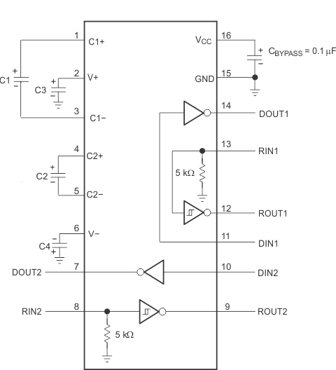
9.2 Typical Application

C3 can be connected to
VCC or GND.
Figure 9-1 Typical
Operating Circuit and Capacitor ValuesTable 9-1 VCC vs Capacitor
Values
| VCC | C1 | C2, C3, C4 | ||
|---|---|---|---|---|
| 3.3 V ± 0.3 V | 0.1 µF | 0.1 µF | ||
| 5 V ± 0.5 V | 0.047 µF | 0.33 µF | ||
| 3 V to 5.5 V | 0.1 µF | 0.47 µF | ||