SCDS247B October 2008 – February 2016 TS12A44513 , TS12A44514 , TS12A44515
PRODUCTION DATA.
- 1 Features
- 2 Applications
- 3 Description
- 4 Revision History
- 5 Pin Configuration and Functions
- 6 Specifications
- 7 Detailed Description
- 8 Application and Implementation
- 9 Power Supply Recommendations
- 10Layout
- 11Device and Documentation Support
- 12Mechanical, Packaging, and Orderable Information
Package Options
Mechanical Data (Package|Pins)
Thermal pad, mechanical data (Package|Pins)
Orderable Information
6 Specifications
6.1 Absolute Maximum Ratings(1)(2)(3)
| MIN | MAX | UNIT | ||||
|---|---|---|---|---|---|---|
| VCC | Supply voltage | –0.3 | 13 | V | ||
| VNC
VNO VCOM |
Analog voltage(4) | –0.3 | VCC + 0.3 | V | ||
| INC
INO ICOM IIN |
Analog current | -20 | 20 | mA | ||
| Peak current (pulsed at 1 ms, 10% duty cycle) | ±30 | mA | ||||
| TA | Operating temperature | –40 | 85 | °C | ||
| PD | Power dissipation | Mounted on JEDEC 4-layer board (JESD 51-7), No airflow, TA = 25°C, TJ = 125°C | PW package | 0.88 | W | |
| Tstg | Storage temperature | –65 | 150 | °C | ||
(1) Stresses beyond those listed under Absolute Maximum Ratings may cause permanent damage to the device. These are stress ratings only, and functional operation of the device at these or any other conditions beyond those indicated under Recommended Operating Conditions is not implied. Exposure to absolute-maximum-rated conditions for extended periods may affect device reliability.
(2) The algebraic convention, whereby the most negative value is a minimum and the most positive value is a maximum
(3) Voltages referenced to GND
(4) Voltages exceeding VCC or GND on any signal terminal are clamped by internal diodes. Limit forward-diode current to maximum current rating.
6.2 ESD Ratings
| VALUE | UNIT | |||
|---|---|---|---|---|
| V(ESD) | Electrostatic discharge | Human-body model (HBM), per ANSI/ESDA/JEDEC JS-001(1) | ±2000 | V |
| Charged-device model (CDM), per JEDEC specification JESD22-C101(2) | ±500 | |||
(1) JEDEC document JEP155 states that 500-V HBM allows safe manufacturing with a standard ESD control process.
(2) JEDEC document JEP157 states that 250-V CDM allows safe manufacturing with a standard ESD control process.
6.3 Recommended Operating Conditions
over operating free-air temperature range (unless otherwise noted)| MIN | MAX | UNIT | ||
|---|---|---|---|---|
| VCC | 2 | 12 | V | |
| VNC, VNO, VCOM, VIN | 0 | VCC | V | |
6.4 Thermal Information
| THERMAL METRIC(1) | TS12A44513, TS12A44514, TS12A44515 | UNIT | ||
|---|---|---|---|---|
| D | PW | |||
| 14 PINS | 14 PINS | |||
| RθJA | Junction-to-ambient thermal resistance | 89.8 | 119.6 | °C/W |
| RθJC(top) | Junction-to-case (top) thermal resistance | 49.6 | 48.4 | |
| RθJB | Junction-to-board thermal resistance | 44.4 | 61.3 | |
| ψJT | Junction-to-top characterization parameter | 13.8 | 5.7 | |
| ψJB | Junction-to-board characterization parameter | 44.1 | 60.7 | |
(1) For more information about traditional and new thermal metrics, see the IC Package Thermal Metrics application report, SPRA953.
6.5 Electrical Characteristics for 5-V Supply(1)
VCC = 4.5 V to 5.5 V, VINH = 2.4 V, VINL = 0.8 V, TA = –40°C to 85°C (unless otherwise noted)| PARAMETER | TEST CONDITIONS | TA | MIN | TYP(2) | MAX | UNIT | ||
|---|---|---|---|---|---|---|---|---|
| ANALOG SWITCH | ||||||||
| VCOM, VNO, VNC | Analog signal range | 0 | VCC | V | ||||
| Ron | ON-state resistance | VCC = 4.5 V, VCOM = 3.5 V, ICOM = 1 mA |
25°C | 12 | 20 | Ω | ||
| Full | 30 | |||||||
| Ron(flat) | ON-state resistance flatness |
VCOM = 1 V, 2 V, 3 V, ICOM = 1 mA |
25°C | 1 | 3 | Ω | ||
| Full | 4 | |||||||
| ΔRon | ON-state resistance matching between channels(5) |
VCC = 4.5 V, ICOM = 5 mA, VNO or VNC = 3 V |
25°C | 3 | Ω | |||
| TMIN to TMAX | 4 | |||||||
| INO(OFF),
INC(OFF) |
NO, NC OFF leakage current(3) |
VCC = 5.5 V, VCOM = 1 V, VNO or VNC = 4.5 V |
25°C | 1 | nA | |||
| Full | 10 | |||||||
| ICOM(OFF) | COM OFF leakage current(3) |
VCC = 5.5 V, VCOM = 1 V, VNO or VNC = 4.5 V |
25°C | 1 | nA | |||
| Full | 10 | |||||||
| ICOM(ON) | COM ON leakage current(3) |
VCC = 5.5 V, VCOM = 4.5 V, VNO or VNC = 4.5 V |
25°C | 1 | nA | |||
| Full | 10 | |||||||
| DIGITAL CONTROL INPUT (IN) | ||||||||
| VIH | Input logic high | Full | 2.4 | VCC | V | |||
| VIL | Input logic low | Full | 0 | 0.8 | V | |||
| IIH, IIL | Input leakage current | VIN = VCC, 0 V | Full | 0.01 | μA | |||
| DYNAMIC | ||||||||
| tON | Turn-on time | see Figure 2 | 25°C | 45 | 100 | ns | ||
| Full | 125 | |||||||
| tOFF | Turn-off time | see Figure 2 | 25°C | 35 | 50 | ns | ||
| Full | 70 | |||||||
| QC | Charge injection(4) | CL = 1 nF, VNO = 0 V, RS = 0 Ω, See Figure 1 |
25°C | –1.5 | pC | |||
| CNO(OFF), CNC(OFF) |
NO, NC OFF capacitance |
f = 1 MHz, See Figure 4 | 25°C | 8 | pF | |||
| CCOM(OFF) | COM OFF capacitance |
f = 1 MHz, See Figure 4 | 25°C | 8 | pF | |||
| CCOM(ON) | COM ON capacitance |
f = 1 MHz, See Figure 4 | 25°C | 19 | pF | |||
| CI | Digital input capacitance | VIN = VCC, 0 V | 25°C | 2 | pF | |||
| BW | Bandwidth | RL = 50 Ω, CL = 15 pF, VNO = 1 VRMS, |
25°C | 530 | MHz | |||
| OISO | OFF isolation | RL = 50 Ω, CL = 15 pF, VNO = 1 VRMS, f = 100 kHz |
25°C | –94 | dB | |||
| THD | Total harmonic distortion | RL = 50 Ω, CL = 15 pF, VNO = 1 VRMS, f = 100 kHz |
25°C | 0.09% | ||||
| SUPPLY | ||||||||
| ICC | Supply Current | VIN = VCC, 0 V | 25°C | 0.05 | μA | |||
| Full | 0.1 | |||||||
(1) The algebraic convention, whereby the most negative value is a minimum and the most positive value is a maximum.
(2) Typical values are at TA = 25°C.
(3) Leakage parameters are 100% tested at maximum-rated hot operating temperature, and are ensured by correlation at 25°C.
(4) Specified by design, not production tested
(5) ΔRON = RON(MAX) – RON(MIN)
6.6 Electrical Characteristics for 12-V Supply(1)
VCC = 11.4 V to 12.6 V, VINH = 5 V, VINL = 0.8 V, TA = –40°C to 85°C (unless otherwise noted)| PARAMETER | TEST CONDITIONS | TA | MIN | TYP(2) | MAX | UNIT | ||
|---|---|---|---|---|---|---|---|---|
| ANALOG SWITCH | ||||||||
| VCOM, VNO, VNC | Analog signal range | 0 | VCC | V | ||||
| Ron | ON-state resistance | VCC = 11.4 V, VCOM = 10 V, ICOM = 1 mA |
25°C | 6.5 | 10 | Ω | ||
| Full | 15 | |||||||
| Ron(flat) | ON-state resistance flatness |
VCC = 11.4 V, VCOM = 2 V, 5 V, 10 V, ICOM = 1 mA |
25°C | 1.5 | 3 | Ω | ||
| Full | 4 | |||||||
| ΔRon | ON-state resistance matching between channels(5) |
VCC = 11.4 V, ICOM = 5 mA, VNO or VNC = 10 V |
25°C | 2.5 | Ω | |||
| TMIN to TMAX | 3 | |||||||
| INO(OFF),
INC(OFF) |
NO, NC OFF leakage current(3) |
VCC = 12.6 V, VCOM = 1 V, VNO or VNC = 10 V |
25°C | 1 | nA | |||
| Full | 10 | |||||||
| ICOM(OFF) | COM OFF leakage current(3) |
VCC = 12.6 V, VCOM = 1 V, VNO or VNC = 10 V |
25°C | 1 | nA | |||
| Full | 10 | |||||||
| ICOM(ON) | COM ON leakage current(3) |
VCC = 12.6 V, VCOM = 10 V, VNO or VNC = 10 V |
25°C | 1 | nA | |||
| Full | 10 | |||||||
| DIGITAL CONTROL INPUT (IN) | ||||||||
| VIH | Input logic high | Full | 5 | VCC | V | |||
| VIL | Input logic low | Full | 0 | 0.8 | V | |||
| IIH, IIL | Input leakage current | VIN = VCC, 0 V | Full | 0.001 | μA | |||
| DYNAMIC | ||||||||
| tON | Turn-on time | See Figure 2 | 25°C | 25 | 75 | ns | ||
| Full | 80 | |||||||
| tOFF | Turn-off time | See Figure 2 | 25°C | 20 | 45 | ns | ||
| Full | 50 | |||||||
| QC | Charge injection(4) | CL = 1 nF, VNO = 0 V, RS = 0 Ω, See Figure 1 |
25°C | –10.5 | pC | |||
| CNO(OFF), CNC(OFF) |
NO, NC OFF capacitance |
f = 1 MHz, See Figure 4 | 25°C | 8 | pF | |||
| CCOM(OFF) | COM OFF capacitance |
f = 1 MHz, See Figure 4 | 25°C | 8 | pF | |||
| CCOM(ON) | COM ON capacitance |
f = 1 MHz, See Figure 4 | 25°C | 21.5 | pF | |||
| CI | Digital input capacitance | VIN = VCC, 0 V | 25°C | 2 | pF | |||
| BW | Bandwidth | RL = 50 Ω, CL = 15 pF, VNO = 1 VRMS, |
25°C | 530 | MHz | |||
| OISO | OFF isolation | RL = 50 Ω, CL = 15 pF, VNO = 1 VRMS, f = 100 kHz |
25°C | –95 | dB | |||
| THD | Total harmonic distortion | RL = 50 Ω, CL = 15 pF, VNO = 1 VRMS, f = 100 kHz |
25°C | 0.07% | ||||
| SUPPLY | ||||||||
| ICC | Supply Current | VIN = VCC, 0 V | 25°C | 0.05 | μA | |||
| Full | 0.2 | |||||||
(1) The algebraic convention, whereby the most negative value is a minimum and the most positive value is a maximum.
(2) Typical Values are at TA = 25°C.
(3) Leakage parameters are 100% tested at maximum-rated hot operating temperature, and are ensured by correlation at 25°C.
(4) Specified by design, not production tested
(5) ΔRON = RON(MAX) – RON(MIN)
6.7 Electrical Characteristics for 3-V Supply(1)
VCC = 3 V to 3.6 V, TA = –40°C to 85°C (unless otherwise noted)| PARAMETER | TEST CONDITIONS | TA | MIN | TYP(2) | MAX | UNIT | ||
|---|---|---|---|---|---|---|---|---|
| ANALOG SWITCH | ||||||||
| VCOM, VNO, VNC | Analog signal range | 0 | VCC | V | ||||
| Ron | ON-state resistance | VCC = 3 V, VCOM = 1.5 V, INO = 1 mA, |
25°C | 20 | 40 | Ω | ||
| Full | 50 | |||||||
| Ron(flat) | ON-state resistance flatness |
VCC = 3 V, VCOM = 1 V, 1.5 V, 2 V, ICOM = 1 mA |
25 °C | 1 | 3 | Ω | ||
| Full | 4 | |||||||
| ΔRon | ON-state resistance matching between channels(5) |
VCC = 2.7 V, ICOM = 5 mA, VNO or VNC = 1.5 V |
25°C | 3.5 | Ω | |||
| TMIN to TMAX | 4.5 | |||||||
| INO(OFF),
INC(OFF) |
NO, NC OFF leakage current(3) |
VCC = 3.6 V, VCOM = 1 V, VNO or VNC = 3 V |
25°C | 1 | nA | |||
| Full | 10 | |||||||
| ICOM(OFF) | COM OFF leakage current(3) |
VCC = 3.6 V, VCOM = 1 V, VNO or VNC = 3 V |
25°C | 1 | nA | |||
| Full | 10 | |||||||
| ICOM(ON) | COM ON leakage current(3) |
VCC = 3.6 V, VCOM = 3 V, VNO or VNC = 3 V |
25°C | 1 | nA | |||
| Full | 10 | |||||||
| DIGITAL CONTROL INPUT (IN) | ||||||||
| VIH | Input logic high | Full | 2.4 | VCC | V | |||
| VIL | Input logic low | Full | 0 | 0.8 | V | |||
| IIH, IIL | Input leakage current | VIN = VCC, 0 V | Full | 0.01 | μA | |||
| DYNAMIC | ||||||||
| tON | Turn-on time(4) | See Figure 2 | 25°C | 70 | 120 | ns | ||
| Full | 175 | |||||||
| tOFF | Turn-off time(4) | See Figure 2 | 25°C | 50 | 80 | ns | ||
| Full | 120 | |||||||
| QC | Charge injection(4) | CL = 1 nF, See Figure 1 | 25°C | –0.5 | pC | |||
| CNO(OFF), CNC(OFF) |
NO, NC OFF capacitance |
f = 1 MHz, See Figure 4 | 25°C | 8 | pF | |||
| CCOM(OFF) | COM OFF capacitance |
f = 1 MHz, See Figure 4 | 25°C | 8 | pF | |||
| CCOM(ON) | COM ON capacitance |
f = 1 MHz, See Figure 4 | 25°C | 17 | pF | |||
| CI | Digital input capacitance | VIN = VCC, 0 V | 25°C | 2 | pF | |||
| BW | Bandwidth | RL = 50 Ω, CL = 15 pF, VNO = 1 VRMS, f = 100 kHz |
25°C | 510 | MHz | |||
| OISO | OFF isolation | RL = 50 Ω, CL = 15 pF, VNO = 1 VRMS, f = 100 kHz |
25°C | –94 | dB | |||
| THD | Total harmonic distortion | RL = 50 Ω, CL = 15 pF, VNO = 1 VRMS, f = 100 kHz |
25°C | 0.27% | ||||
| SUPPLY | ||||||||
| ICC | Supply Current | VIN = VCC, 0 V | 25°C | 0.05 | μA | |||
| Full | 0.2 | |||||||
(1) The algebraic convention, whereby the most negative value is a minimum and the most positive value is a maximum.
(2) Typical values are at TA = 25°C.
(3) Leakage parameters are 100% tested at maximum-rated hot operating temperature, and are ensured by correlation at 25°C.
(4) Specified by design, not production tested
(5) ΔRON = RON(MAX) – RON(MIN)
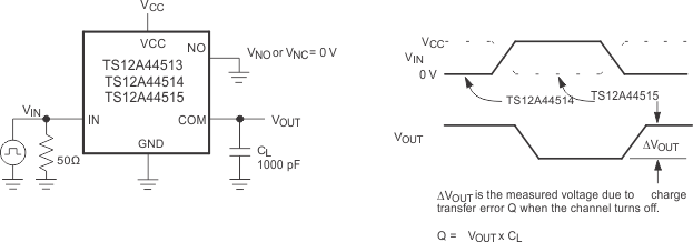 Figure 1. Charge Injection
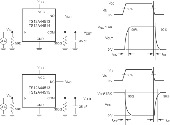 Figure 2. Switching Times
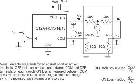 Figure 3. Off Isolation and On Loss
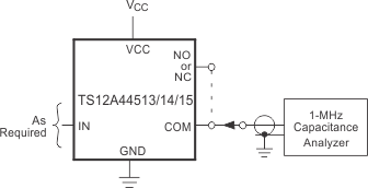 Figure 4. NO, NC, and COM Capacitance
6.8 Typical Characteristics
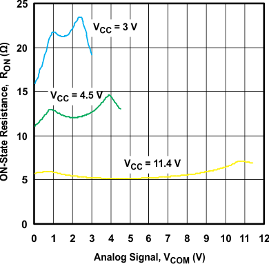 Figure 5. RON vs VCOM (TA = 25°C)
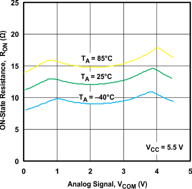 Figure 7. RON vs VCOM (VCC = 4.5 V)
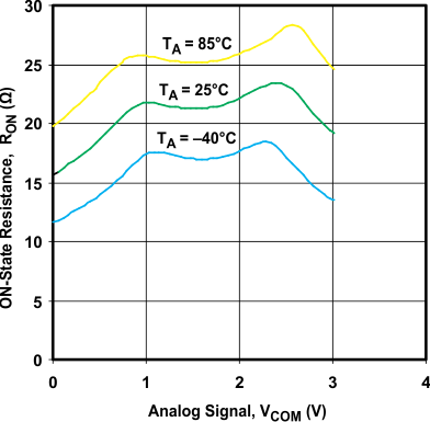 Figure 6. RON vs VCOM (VCC = 3 V)
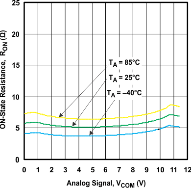 Figure 8. RON vs VCOM (VCC = 11.4 V)