SCDS430A December 2020 – May 2021 TS3DV642-Q1
PRODUCTION DATA
- 1 Features
- 2 Applications
- 3 Description
- 4 Revision History
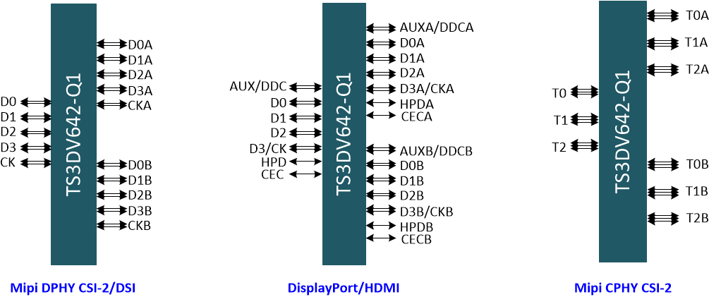
- 5 Pin Configuration and Functions
- 6 Specifications
- 7 Parameter Measurement Information
- 8 Detailed Description
- 9 Application and Implementation
- 10Power Supply Recommendations
- 11Layout
- 12Device and Documentation Support
- 13Mechanical, Packaging, and Orderable Information
Package Options
Refer to the PDF data sheet for device specific package drawings
Mechanical Data (Package|Pins)
- RUA|42
Thermal pad, mechanical data (Package|Pins)
Orderable Information
3 Description
The TS3DV642-Q1 is an analog high-speed bidirectional passive switch in mux or demux configurations that works for many high-speed differential interfaces with data rates up to 6 Gbps. It is suited for many applications including HDMI 1.4 / 2.0, DisplayPort 1.4 and Mipi DPHY / CPHY DSI / CSI-2. The TS3DV642-Q1 supports both differential and single-ended signaling - virtually compatible to most standard and non standard interfaces. The dynamic characteristics of the TS3DV642-Q1 allows high-speed switching with minimal attenuation to the signal eye diagram, and with very little added jitter. The device's silicon design is optimized for excellent frequency response at higher frequency spectrum of the signals. The device supports differential signaling with common mode voltage range (CMV) of 0 to 3.6 V. The device also supports 0 - 5.5 V single-ended CMOS signals.
The TS3DV642-Q1 consumes very low active power of 45 μA. The device also offers a power-down mode, in which all channels become Hi-Z and the device operates with minimal power.
| PART NUMBER | PACKAGE | BODY SIZE (NOM) |
|---|---|---|
| TS3DV642-Q1 | WQFN (42) | 3.50 mm x 9.00 mm |