SCDS261H March 2008 – June 2017 TS5A22364
PRODUCTION DATA.
- 1 Features
- 2 Applications
- 3 Description
- 4 Revision History
- 5 Pin Configuration and Functions
- 6 Specifications
- 7 Parameter Measurement Information
- 8 Detailed Description
- 9 Application and Implementation
- 10Power Supply Recommendations
- 11Layout
- 12Device and Documentation Support
- 13Mechanical, Packaging, and Orderable Information
Package Options
Mechanical Data (Package|Pins)
Thermal pad, mechanical data (Package|Pins)
- DRC|10
Orderable Information
8 Detailed Description
8.1 Overview
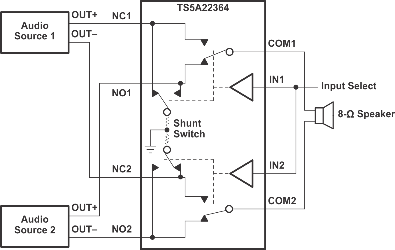
The TS5A22364 is a bidirectional 2-channel, single-pole, double-throw (SPDT) analog switch designed to operate from 2.3-V to 5.5-V power supply. The device features negative signal swing capability that allows signals below ground to pass through the switch without distortion. Additionally, the TS5A22364 includes an internal shunt switch, which automatically discharges any capacitance at the NC or NO terminals when they are not connected to COM. Discharging the capacitance reduces the audible click and pop noise when switching between two sources. The break-before-make feature prevents signal distortion during the transferring of a signal from one path to another. Low ON-state resistance, excellent channel-to-channel ON-state resistance matching, and minimal total harmonic distortion (THD) performance are ideal for audio applications.
8.2 Functional Block Diagram

8.3 Feature Description
8.3.1 Click and Pop Reduction
The shunt resistors in the TS5A22364 automatically discharge any capacitance at the NC or NO terminals when they are not connected to COM. This reduces the audible click-and-pop sounds that occur when switching between audio sources. Audible clicks and pops are caused when a step DC voltage is switched into the speaker. By automatically discharging the side that is not connected, any residual DC voltage is removed, thereby reducing the clicks and pops.
8.3.2 Negative Signal Swing Capability
The TS5A22364 2-channel SPDT switch features negative signal capability that allows signals below ground to pass through without distortion. These analog switches operate from a single 2.3-V to 5.5-V supply. The input and output signal swing of the device is dependant of the supply voltage VCC. The device passes signals as high as VCC and as low as VCC – 5.5 V, including signals below ground with minimal distortion. The OFF state signal path (either NC or NO) during the operation of TS5A22364 cannot handle negative DC voltage
Table 1 shows the input/output signal swing the user can get with different supply voltages.
Table 1. Input/Output Signal Swing
| SUPPLY VOLTAGE, VCC | MINIMUM VNC, VNO, VCOM = VCC - 5.5 V |
MAXIMUM VNC, VNO, VCOM = VCC |
|---|---|---|
| ON-STATE SIGNAL PATH | ||
| 5.5 V | 0 V | 5.5 V |
| 4.5 V | –1.0 V | 4.5 V |
| 3.6 V | –1.9 V | 3.6 V |
| 3.0 V | –2.5 V | 3.0 V |
| 2.7 V | –2.8 V | 2.7 V |
| 2.3 V | -3.2 V | 2.3 V |
8.4 Device Functional Modes
The function table for TS5A22364 is shown in Table 2.
Table 2. Function Table
| IN | NC TO COM, COM TO NC |
NO TO COM, COM TO NO |
|---|---|---|
| L | ON | OFF |
| H | OFF | ON |