SCDS261H March 2008 – June 2017 TS5A22364
PRODUCTION DATA.
- 1 Features
- 2 Applications
- 3 Description
- 4 Revision History
- 5 Pin Configuration and Functions
- 6 Specifications
- 7 Parameter Measurement Information
- 8 Detailed Description
- 9 Application and Implementation
- 10Power Supply Recommendations
- 11Layout
- 12Device and Documentation Support
- 13Mechanical, Packaging, and Orderable Information
Package Options
Mechanical Data (Package|Pins)
Thermal pad, mechanical data (Package|Pins)
- DRC|10
Orderable Information
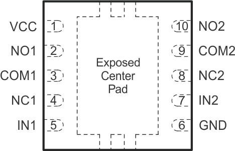
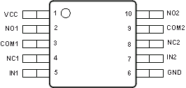
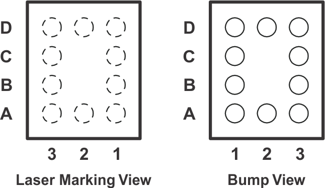
5 Pin Configuration and Functions
DRC Package
10-Pin VSON
Top View

*The exposed center pad, if used, must be connected as a secondary GND or left electrically open.
DGS Package
10-Pin VSSOP
Top View

YZP Package
10-Pin DSBGA
Top View

Pin Functions
| PIN | TYPE | DESCRIPTION | ||
|---|---|---|---|---|
| NAME | DRC / DGS | YZP | ||
| VCC | 1 | A2 | — | Power Supply |
| NO1 | 2 | A3 | I/O | Normally Open (NO) signal path, Switch 1 |
| COM1 | 3 | B3 | I/O | Common signal path, Switch 1 |
| NC1 | 4 | C3 | I/O | Normally Closed (NC) signal path, Switch 1 |
| IN1 | 5 | D3 | I | Digital control pin to connect COM1 to NO1, Switch 1 |
| GND | 6 | D2 | — | Ground |
| IN2 | 7 | D1 | I | Digital control pin to connect COM2 to NO2, Switch 2 |
| NC2 | 8 | C1 | I/O | Normally Closed (NC) signal path, Switch 2 |
| COM2 | 9 | B1 | I/O | Common signal path, Switch 2 |
| NO2 | 10 | A1 | I/O | Normally Open (NO) signal Path, Switch 2 |