SBAS484B September 2010 – December 2016 TSC2014
PRODUCTION DATA.
- 1 Features
- 2 Applications
- 3 Description
- 4 Revision History
- 5 Pin Configuration and Functions
-
6 Electrical Specifications
- 6.1 Absolute Maximum Ratings
- 6.2 ESD Ratings
- 6.3 Thermal Information
- 6.4 Recommended Operating Conditions
- 6.5 Electrical Characteristics
- 6.6 Timing Requirements for : I2C Standard Mode (fSCL = 100 kHz)
- 6.7 Timing Requirements for : I2C Fast Mode (fSCL = 400 kHz)
- 6.8 Timing Requirements for : I2C High-Speed Mode (fSCL = 1.7 MHz)
- 6.9 Timing Requirements for : I2C High-Speed Mode (fSCL = 3.4 MHz)
- 6.10 Timing Information
- 6.11 Typical Characteristics
-
7 Detailed Description
- 7.1 Overview
- 7.2 Functional Block Diagram
- 7.3 Feature Description
- 7.4 Device Functional Modes
- 7.5 Programming
- 7.6
Register Maps
- 7.6.1 R/W
- 7.6.2 Control Byte 0
- 7.6.3 Control Byte 1
- 7.6.4 Communication Protocol
- 7.6.5 Configuration Register 2
- 7.6.6 Converter Function Select Register
- 7.6.7 Data Registers
- 8 Application and Implementation
- 9 Power Supply Recommendations
- 10Layout
- 11Device and Documentation Support
- 12Mechanical, Packaging, and Orderable Information
Package Options
Mechanical Data (Package|Pins)
- YZG|12
Thermal pad, mechanical data (Package|Pins)
Orderable Information
8 Application and Implementation
NOTE
Information in the following applications sections is not part of the TI component specification, and TI does not warrant its accuracy or completeness. TI’s customers are responsible for determining suitability of components for their purposes. Customers should validate and test their design implementation to confirm system functionality.
8.1 Application Information
Communication with the TSC2014 is done via an I2C serial interface. The TSC2014 is an I2C slave device; therefore, data are shifted into or out of the TSC2014 under the control of the host microprocessor, which also provides the serial data clock.
Control of the TSC2014 and its functions is accomplished by writing to different registers in the TSC2014. A simple command protocol (compatible with I2C) is used to address these registers. This protocol can be an I2C write-addressing followed by multiple control bytes, or multiple combinations of control/data bytes to be written into different registers (two bytes each). Reading from registers is performed by writing an I2C read-addressing to the TSC, followed by one or multiple sequential reads from the registers.
The address of the register to be read can be written in TSC Control Byte 0 with the register address and read-bit (as described in the previous paragraph), and serves as a pointer to the register map where the first read starts. This designated register address is static; there is no need to write a register address again unless it is overwritten by a new register address, or if the TSC is reset (by a software reset or by the RESET pin).
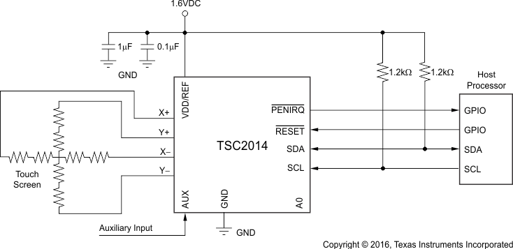
The measurement result is placed in the TSC2014 registers and may be read by the host at any time. This preprocessing frees up the host so that resources can be redirected for more critical tasks. Two optional signals are also available from the TSC2014 to indicate that data are available for the host to read. PINTDAV is a programmable interrupt/status output pin. When PINTDAV is programmed as a DAV output, it indicates that an A/D conversion has completed and that data are available. When this pin is programmed as a PENIRQ output, it indicates that a touch has been detected on the touch screen. The status register of the TSC2014 provides an extended status reading including the state of DAV and PENIRQ without the cost of any dedicated pin. Figure 45 shows a typical application of the TSC2014.
8.2 Typical Application
 Figure 45. Typical Circuit Configuration
8.2.1 Design Requirements
For this design example, use the parameters shown in Table 25.
Table 25. Design Parameters
| PARAMETER | VALUE |
|---|---|
| Power Supply | 1.6 V |
| Reset | VIH ≥ 1.12 |
| VIL ≤ 0.48 | |
| Touch Panel | 4 Wire |
8.2.2 Detailed Design Procedure
8.2.2.1 Auxiliary and Temperature Measurement
The TSC2014 can measure the voltage from the auxiliary input (AUX) and from the internal temperature sensor. Applications for the AUX can include external temperature sensing, ambient light monitoring for controlling backlighting, or sensing the current drawn from batteries. There are two converter functions that can be used for the measurement of the AUX:
- Non-continuous AUX measurement shown in Figure 46 (converter function select bits C[3:0] = Control Byte 1 D[6:3] = 0101); or
- Continuous AUX Measurement shown in Figure 47 (converter function select bits C[3:0] = Control Byte 1 D[6:3] = 1000).
See Table 9 for more information on the converter function select bits.
There are also two converter functions for the measurement of the internal temperature sensor:
- TEMP1 measurement (converter function select bits C[3:0] = Control Byte 1 D[6:3] = 0110); or
- TEMP2 measurement (converter function select bits C[3:0] = Control Byte 1 D[6:3] = 0111).
See Table 9 for more information on the converter function select bits.
For the detailed calculation of the internal temperature sensor, see the section. These two converter functions have the same timing as the non-continuous AUX measurement operation as shown in Figure 46; therefore, Equation 12 can also be used for internal temperature sensor measurement. The time needed to make a non-continuous auxiliary measurement or an internal temperature sensor measurement is given by:

Where:
OH3 = overhead time #3 = 3.5 internal clock cycles.
 Figure 46. Non-Touch Screen, Non-Continuous AUX Measurement
The time needed to make continuous auxiliary measurement is given by:

 Figure 47. Non-Touch Screen, Continuous AUX Measurement