SLDS251A December 2019 – May 2022 TUSS4470
PRODUCTION DATA
- 1 Features
- 2 Applications
- 3 Description
- 4 Revision History
- 5 Pin Configuration and Functions
-
6 Specifications
- 6.1 Absolute Maximum Ratings
- 6.2 ESD Ratings
- 6.3 Recommended Operating Conditions
- 6.4 Thermal Information
- 6.5 Power-Up Characteristics
- 6.6 Transducer Drive
- 6.7 Receiver Characteristics
- 6.8 Echo Interrupt Comparator Characteristics
- 6.9 Digital I/O Characteristics
- 6.10 Switching Characteristics
- 6.11 Typical Characteristics
- 7 Detailed Description
- 8 Application and Implementation
- 9 Power Supply Recommendations
- 10Layout
- 11Device and Documentation Support
- 12Mechanical, Packaging, and Orderable Information
Package Options
Mechanical Data (Package|Pins)
- RTJ|20
Thermal pad, mechanical data (Package|Pins)
- RTJ|20
Orderable Information
6.11 Typical Characteristics
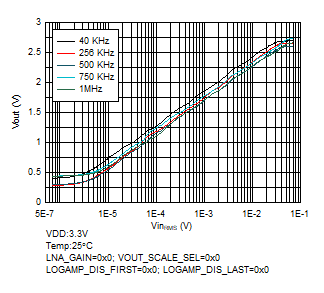 Figure 6-1 Receive Signal Path Transfer Function for VDD = 3.3 V
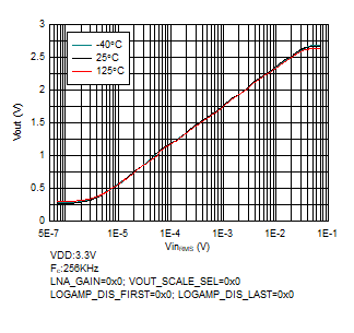 Figure 6-3 Receive Signal Path Transfer Function Across Temperature
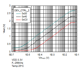 Figure 6-5 Receive Signal Path Transfer Function for Various Logamp Stages Disabled
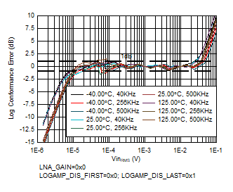 Figure 6-7 Receive Signal Path Log Conformance Error With Last Stage Disabled
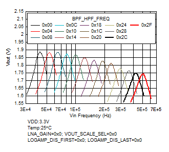 Figure 6-9 Receive Signal Path Bandpass Filter Transfer Function
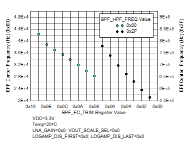 Figure 6-11 Receive Signal Path Bandpass Filter Center Frequency Trim
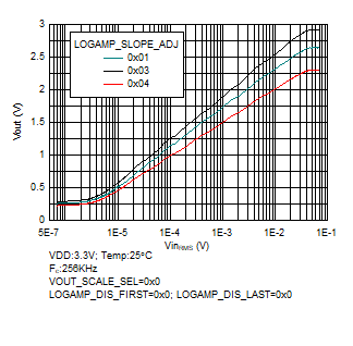 Figure 6-13 Receive Signal Path Transfer Function for Various Slope Adjustments
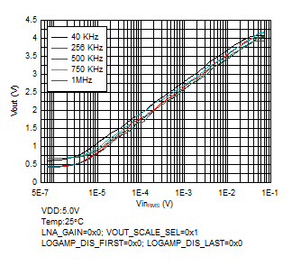 Figure 6-2 Receive Signal Path Transfer Function for VDD = 5 V
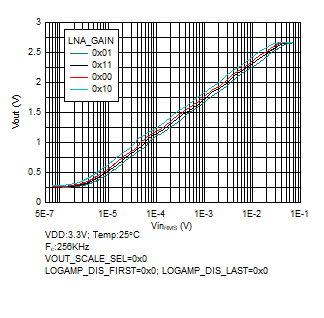 Figure 6-4 Receive Signal Path Transfer Function Across LNA Gain
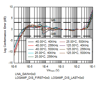 Figure 6-6 Receive Signal Path Log Conformance Error With All Stages Enabled
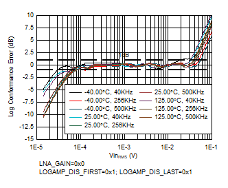 Figure 6-8 Receive Signal Path Log Conformance Error With First and Last Stage Disabled
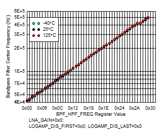
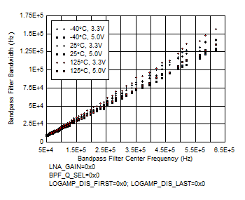 Figure 6-12 Receive Signal Path Bandpass Filter Bandwidth for Various Center Frequency Settings
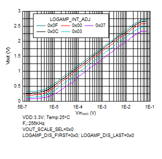 Figure 6-14 Receive Signal Path Transfer Function for Various Intercept Adjustments