SCES639E January 2007 – March 2023 TXB0101
PRODUCTION DATA
- 1 Features
- 2 Applications
- 3 Description
- 4 Revision History
- 5 Pin Configuration and Functions
-
6 Specification
- 6.1 Absolute Maximum Ratings
- 6.2 ESD Ratings
- 6.3 Recommended Operating Conditions
- 6.4 Thermal Information
- 6.5 Electrical Characteristics
- 6.6 Timing Requirements, VCCA = 1.2 V
- 6.7 Timing Requirements, VCCA = 1.5 V ± 0.1 V
- 6.8 Timing Requirements, VCCA = 1.8 V ± 0.15 V
- 6.9 Timing Requirements, VCCA = 2.5 V ± 0.2 V
- 6.10 Timing Requirements, VCCA = 3.3 V ± 0.3 V
- 6.11 Switching Characteristics, VCCA = 1.2 V
- 6.12 Switching Characteristics, VCCA = 1.5 V ± 0.1 V
- 6.13 Switching Characteristics, VCCA = 1.8 V ± 0.15 V
- 6.14 Switching Characteristics, VCCA = 2.5 V ± 0.2 V
- 6.15 Switching Characteristics, VCCA = 3.3 V ± 0.3 V
- 6.16 Operating Characteristics
- 6.17 Typical Characteristics
- 7 Detailed Description
- 8 Application and Implementation
- 9 Device and Documentation Support
- 10Mechanical, Packaging, and Orderable Information
Package Options
Mechanical Data (Package|Pins)
Thermal pad, mechanical data (Package|Pins)
- DCK|6
Orderable Information
3 Description
This 1-bit noninverting translator uses two separate configurable power-supply rails. The A port is designed to track VCCA. VCCA accepts any supply voltage from 1.2 V to 3.6 V. The B port is designed to track VCCB. VCCB accepts any supply voltage from 1.65 V to 5.5 V. This allows for universal low-voltage bidirectional translation between any of the 1.2-V, 1.5-V, 1.8-V, 2.5-V, 3.3-V, and 5-V voltage nodes. VCCA should not exceed VCCB.
When the output-enable (OE) input is low, all outputs are placed in the high-impedance state.
This device is fully specified for partial-power-down applications using Ioff. The Ioff circuitry disables the outputs, preventing damaging current backflow through the device when it is powered down.
To ensure the high-impedance state during power up or power down, OE should be tied to GND through a pulldown resistor; the minimum value of the resistor is determined by the current-sourcing capability of the driver.
NanoFree™ package technology is a major breakthrough in IC packaging concepts, using the die as the package.
| PART NUMBER | PACKAGE(1) | BODY SIZE (NOM) |
|---|---|---|
| TXB0101 | SOT-23 (DBV) (6) | 2.90 mm × 1.60 mm |
| SC70 (DCK) (6) | 2.00 mm × 1.25 mm | |
| SOT (DRL) (6) | 1.60 mm × 1.20 mm | |
| DSBGA (YZP) (6) | 0.90 mm × 1.40 mm |
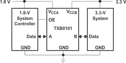
 Typical Operating Circuit