SLUS336A June 1998 – December 2016 UC1854 , UC2854 , UC3854
PRODUCTION DATA.
- 1 Features
- 2 Applications
- 3 Description
- 4 Revision History
- 5 Device Comparison Table
- 6 Pin Configuration and Functions
- 7 Specifications
- 8 Detailed Description
- 9 Application and Implementation
- 10Power Supply Recommendations
- 11Layout
- 12Device and Documentation Support
- 13Mechanical, Packaging, and Orderable Information
Package Options
Refer to the PDF data sheet for device specific package drawings
Mechanical Data (Package|Pins)
- DW|16
- N|16
Thermal pad, mechanical data (Package|Pins)
- DW|16
Orderable Information
9 Application and Implementation
NOTE
Information in the following applications sections is not part of the TI component specification, and TI does not warrant its accuracy or completeness. TI’s customers are responsible for determining suitability of components for their purposes. Customers should validate and test their design implementation to confirm system functionality.
9.1 Application Information
The UC3854 control IC is generally applicable to the control of AC-DC power supplies that require Active Power Factor Correction off Universal AC line. Applications using this IC generally meets the Class D equipment input current harmonics standards per EN61000-3-2. This standard applies to equipment with rated powers higher than 75 W.
Performance of the UC3854 Power Factor correction IC in a 250-W application example has been evaluated using a precision PFC and THD instrument. The result was a power factor of 0.999 and Total Harmonic Distortion (THD) of 3.81%, measured to the 50th line frequency harmonic at nominal line and full load.
9.2 Typical Application
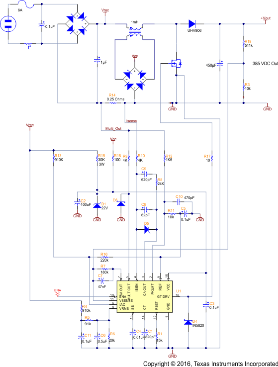
The circuit of Figure 9 shows a typical application of the UC3854 as a preregulator with high power factor and efficiency. The assembly consists of two distinct parts: the control circuit centering on the UC3854 and the power section.
The power section is a boost converter, with the inductor operating in continuous mode. In this mode, the duty cycle is dependent on the ratio between input and output voltages; also, the input current has low switching-frequency ripple, which means that the line noise is low. Furthermore, the output voltage must be higher than the peak value of the highest expected AC line voltage, and all components must be rated accordingly.
At full load, this preregulator exhibits a power factor of 0.99 at any power line voltage from 80 V to 260 VRMS. This same circuit is used at higher power levels with minor modifications to the power stage. See Optimizing Performance in UC3854 Power Factor Correction Applications and UC3854 Controlled Power Factor Correction Circuit Design.

9.2.1 Design Requirements
For this design example, use the parameters listed in Table 1 as the input parameters.
Table 1. Design Parameters
| DESIGN PARAMETER | MIN | TYP | MAX | UNIT | |
|---|---|---|---|---|---|
| VIN | RMS input voltage | 80 | 260 | VRMS | |
| VOUT | Output voltage | 390 | V | ||
| fLine | AC line frequency | 47 | 65 | Hz | |
| POUT(max) | Maximum output power | 250 | W | ||
9.2.2 Detailed Design Procedure
In the control section, the UC3854 provides PWM pulses (GTDRV) to the power MOSFET gate. The duty cycle of this output is simultaneously controlled by four separate inputs to the chip.
Table 2. Output Duty Cycle
| INPUT PIN | FUNCTION |
|---|---|
| VSENSE | Output DC voltage |
| IAC | Line voltage waveform |
| ISENSE, MULTOUT | Line current |
| VRMS | RMS line voltage |
Additional controls of an auxiliary nature are provided. They are intended to protect the switching power MOSFETS from certain transient conditions.
Table 3. Additional Controls of the Output Duty Cycle
| INPUT PIN | FUNCTION |
|---|---|
| ENA | Startup delay |
| SS | Soft start |
| PKLMT | Maximum current limit |
9.2.2.1 Protection Inputs
ENA (Enable): The ENA input must reach 2.5 V before the VREF and GTDRV outputs are enabled. This provides a means to shut down the gate in case of trouble, or to add a time delay at power up. A hysteresis gap of 200 mV is provided at this terminal to prevent erratic operation. Undervoltage protection is provided directly at VCC, where the on and off thresholds are 16 V and 10 V. If the ENA input is unused, it must be pulled up to VCC through a current-limiting resistor of 100 kΩ.
SS (Soft Start): The voltage at SS pin reduces the reference voltage used by the error amplifier to regulate the output DC voltage. With SS open, the reference voltage is typically 7.5 V. An internal current source delivers approximately 14 mA from SS. Thus a capacitor (CSS) connected between SS and ground charges linearly from 0 V to 7.5 V in [0.54 × CSS (µF)] s.
PKLMT (Peak Current Limit): Use PKLIM to establish the highest value of current to be controlled by the power MOSFET. With the resistor divider values shown in Figure 9, the 0-V threshold at PKLIM is reached when the voltage drop across the 0.25-Ω current-sense resistor is 7.5 V × 2 k / 10 k = 1.5 V, corresponding to 6 A. TI recommends a bypass capacitor from PKLIM to GND to filter out very high frequency noise.
9.2.2.2 Control Inputs
VSENSE (Output DC Voltage Sense): The threshold voltage for the VSENSE input is 7.5 V and the input bias current is typically 50 nA. The values shown in Figure 9 are for an output voltage of 400-V DC. In this circuit, the voltage amplifier operates with a constant low-frequency gain for minimum output excursions. The 47-nF feedback capacitor places a 15-Hz pole in the voltage loop that prevents 120-Hz ripple from propagating to the input current.
IAC (Line Waveform): To force the line current waveshape to follow the line voltage, a sample of the power line voltage in waveform is introduced at IAC. This signal is multiplied by the output of the voltage amplifier in the internal multiplier to generate a reference signal for the current control loop.
This input is not a voltage, but a current (hence IAC), and is set up by the 220-kΩ and 910-kΩ resistive divider (see Figure 12). The voltage at IAC is internally held at 6 V, and the two resistors are chosen so that the current flowing into IAC varies from zero (at each zero-crossing) to about 400 µA at the peak of the waveshape. The following formulas are used to calculate these resistors:

where
- VPK is the peak line voltage

ISENSE and MULTOUT (Line Current): The voltage drop across the 0.25-Ω current-sense resistor is applied to ISENSE and MULTOUT as shown. The current-sense amplifier also operates with high low-frequency gain, but unlike the voltage amplifier, it is set up to give the current-control loop a very wide bandwidth. This bandwidth enables the line current to follow the line voltage as closely as possible. In the present example, this amplifier has a zero at about 500 Hz, and a gain of about 18 dB thereafter.
VRMS (RMS Line Voltage): An important feature of the UC3854 preregulator is that it operates with a three-to-one range of input line voltages, covering everything from low line in the US (85 VAC) to high line in Europe (255 VAC). This is done using line feedforward, which keeps the input power constant with varying input voltage (assuming constant load power). To do this, the multiplier divides the line current by the square of the RMS value of the line voltage. The voltage applied to VRMS, proportional to the average of the rectified line voltage and proportional to the RMS value, is squared in the UC3854, and then used as a divisor by the multiplier block. The multiplier output, at MULTOUT, is a current that increases with the current at IAC and the voltage at VAOUT, and decreases with the square of the voltage at VRMS.
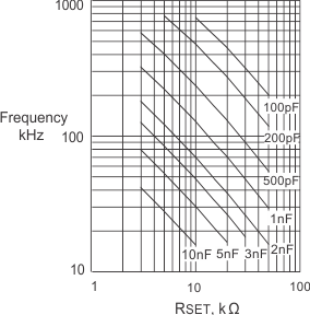
PWM Frequency: The PWM oscillator frequency in Figure 9 is 100 kHz. This value is determined by CT at pin CT and RSET at pin RSET. RSET must be chosen first because it affects the maximum value of IMULT according to the equation Equation 4.

This effectively sets a maximum PWM-controlled current. With RSET = 15 k,

Also note that the multiplier output current never exceeds twice IAC.
With the 4-kΩ resistor from MULTOUT to the 0.25-Ω current-sense resistor, the maximum current in the current-sense resistor is:

Having thus selected RSET, the current sense resistor, and the resistor from MULTOUT to the current sense resistor, calculate CT for the desired PWM oscillator frequency from Equation 7.

9.2.3 Application Curves

 Figure 11. Oscillator Frequency vs RSET and CT