SLUS336A June 1998 – December 2016 UC1854 , UC2854 , UC3854
PRODUCTION DATA.
- 1 Features
- 2 Applications
- 3 Description
- 4 Revision History
- 5 Device Comparison Table
- 6 Pin Configuration and Functions
- 7 Specifications
- 8 Detailed Description
- 9 Application and Implementation
- 10Power Supply Recommendations
- 11Layout
- 12Device and Documentation Support
- 13Mechanical, Packaging, and Orderable Information
Package Options
Refer to the PDF data sheet for device specific package drawings
Mechanical Data (Package|Pins)
- DW|16
- N|16
Thermal pad, mechanical data (Package|Pins)
- DW|16
Orderable Information
11 Layout
11.1 Layout Guidelines
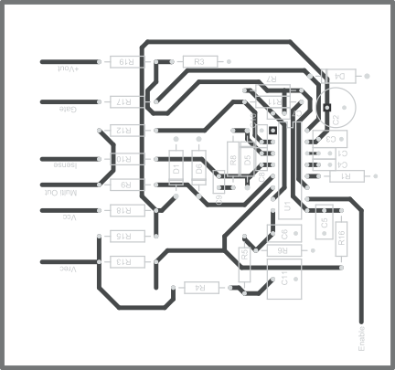
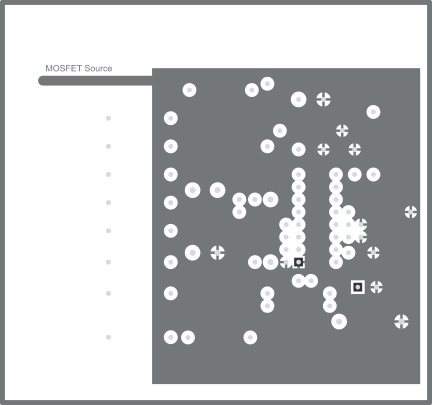
Figure 12 and Figure 13 show good layout practice. The timing capacitor (C1) and bypass capacitors for VCC and VREF (C3 and C5) must be connected directly from their respective pins to GND through the shortest route. Ensure that the ISEN and MULTOUT pins do not drop more than 0.5 V below the GND pin; accomplished by connecting a Schottky diode (D6) between GND and MULTOUT pins. The local controller GND must be connected to the power circuit at a single point between the source of the power MOSFET and the current sense resistor (R14). The power trace running between the power MOSFET source and current sense resistor (R14) must be kept short. Traces from the upper terminals of R9 and R10 must run directly to each side of the current sense resistor and not be shared with any other signal.
To minimize the possiblity of interference caused by magnetic coupling from the boost inductor, the device must be located at least 1 in. away from the boost inductor. TI recommends the device not be placed underneath magnetic elements.
11.2 Layout Example
 Figure 12. Layout Diagram (Top View)
 Figure 13. Layout Diagram (Bottom View)