SLUSDS3A March 2020 – January 2024 UCC21739-Q1
PRODUCTION DATA
- 1
- 1 Features
- 2 Applications
- 3 Description
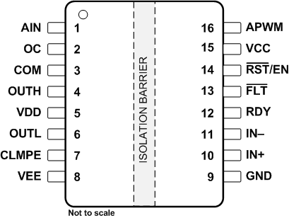
- 4 Pin Configuration and Functions
-
5 Specifications
- 5.1 Absolute Maximum Ratings
- 5.2 ESD Ratings
- 5.3 Recommended Operating Conditions
- 5.4 Thermal Information
- 5.5 Power Ratings
- 5.6 Insulation Specifications
- 5.7 Safety-Related Certifications
- 5.8 Safety Limiting Values
- 5.9 Electrical Characteristics
- 5.10 Switching Characteristics
- 5.11 Insulation Characteristics Curves
- 5.12 Typical Characteristics
- 6 Parameter Measurement Information
-
7 Detailed Description
- 7.1 Overview
- 7.2 Functional Block Diagram
- 7.3
Feature Description
- 7.3.1 Power Supply
- 7.3.2 Driver Stage
- 7.3.3 VCC and VDD Undervoltage Lockout (UVLO)
- 7.3.4 Active Pulldown
- 7.3.5 Short Circuit Clamping
- 7.3.6 External Active Miller Clamp
- 7.3.7 Overcurrent and Short Circuit Protection
- 7.3.8 2-Level Turn-off
- 7.3.9 Fault ( FLT, Reset and Enable ( RST/EN)
- 7.3.10 Isolated Analog to PWM Signal Function
- 7.4 Device Functional Modes
-
8 Applications and Implementation
- 8.1 Application Information
- 8.2
Typical Application
- 8.2.1 Design Requirements
- 8.2.2
Detailed Design Procedure
- 8.2.2.1 Input filters for IN+, IN- and RST/EN
- 8.2.2.2 PWM Interlock of IN+ and IN-
- 8.2.2.3 FLT, RDY and RST/EN Pin Circuitry
- 8.2.2.4 RST/EN Pin Control
- 8.2.2.5 Turn-On and Turn-Off Gate Resistors
- 8.2.2.6 External Active Miller Clamp
- 8.2.2.7 Overcurrent and Short Circuit Protection
- 8.2.2.8 Isolated Analog Signal Sensing
- 8.2.2.9 Higher Output Current Using an External Current Buffer
- 8.2.3 Application Curves
- 9 Power Supply Recommendations
- 10Layout
- 11Device and Documentation Support
- 12Revision History
- 13Mechanical, Packaging, and Orderable Information
Package Options
Mechanical Data (Package|Pins)
- DW|16
Thermal pad, mechanical data (Package|Pins)
- DW|16
Orderable Information
3 Description
The UCC21739-Q1 is a galvanic isolated single channel gate drivers designed for SiC MOSFETs and IGBTs up to 900V DC operating voltage with advanced protection features, best-in-class dynamic performance and robustness. UCC21739-Q1 has up to ±10A peak source and sink current.
The input side is isolated from the output side with SiO2 capacitive isolation technology, supporting up to 636VRMS working voltage, 6kVPK surge immunity basic isolation with longer than 40 years isolation barrier life, as well as providing low part-to-part skew, and >150V/ns common mode noise immunity (CMTI).
The UCC21739-Q1 includes the state-of-art protection features, such as fast overcurrent and short circuit detection, shunt current sensing support, fault reporting, active miller clamp, and input and output side power supply UVLO to optimize SiC and IGBT switching behavior and robustness. The isolated analog to PWM sensor can be utilized for easier temperature or voltage sensing, further increasing the drivers' versatility and simplifying the system design effort, size and cost.
| PART NUMBER | PACKAGE(1) | BODY SIZE (NOM) |
|---|---|---|
| UCC21739-Q1 | DW (SOIC-16) | 10.3 mm × 7.5 mm |