SLUSDS3A March 2020 – January 2024 UCC21739-Q1
PRODUCTION DATA
- 1
- 1 Features
- 2 Applications
- 3 Description
- 4 Pin Configuration and Functions
-
5 Specifications
- 5.1 Absolute Maximum Ratings
- 5.2 ESD Ratings
- 5.3 Recommended Operating Conditions
- 5.4 Thermal Information
- 5.5 Power Ratings
- 5.6 Insulation Specifications
- 5.7 Safety-Related Certifications
- 5.8 Safety Limiting Values
- 5.9 Electrical Characteristics
- 5.10 Switching Characteristics
- 5.11 Insulation Characteristics Curves
- 5.12 Typical Characteristics
- 6 Parameter Measurement Information
-
7 Detailed Description
- 7.1 Overview
- 7.2 Functional Block Diagram
- 7.3
Feature Description
- 7.3.1 Power Supply
- 7.3.2 Driver Stage
- 7.3.3 VCC and VDD Undervoltage Lockout (UVLO)
- 7.3.4 Active Pulldown
- 7.3.5 Short Circuit Clamping
- 7.3.6 External Active Miller Clamp
- 7.3.7 Overcurrent and Short Circuit Protection
- 7.3.8 2-Level Turn-off
- 7.3.9 Fault ( FLT, Reset and Enable ( RST/EN)
- 7.3.10 Isolated Analog to PWM Signal Function
- 7.4 Device Functional Modes
-
8 Applications and Implementation
- 8.1 Application Information
- 8.2
Typical Application
- 8.2.1 Design Requirements
- 8.2.2
Detailed Design Procedure
- 8.2.2.1 Input filters for IN+, IN- and RST/EN
- 8.2.2.2 PWM Interlock of IN+ and IN-
- 8.2.2.3 FLT, RDY and RST/EN Pin Circuitry
- 8.2.2.4 RST/EN Pin Control
- 8.2.2.5 Turn-On and Turn-Off Gate Resistors
- 8.2.2.6 External Active Miller Clamp
- 8.2.2.7 Overcurrent and Short Circuit Protection
- 8.2.2.8 Isolated Analog Signal Sensing
- 8.2.2.9 Higher Output Current Using an External Current Buffer
- 8.2.3 Application Curves
- 9 Power Supply Recommendations
- 10Layout
- 11Device and Documentation Support
- 12Revision History
- 13Mechanical, Packaging, and Orderable Information
Package Options
Mechanical Data (Package|Pins)
- DW|16
Thermal pad, mechanical data (Package|Pins)
- DW|16
Orderable Information
8.2.2.8.2 Isolated DC Bus Voltage Sensing
The AIN to APWM channel may be used for other applications such as the DC-link voltage sensing, as shown in Figure 8-16. The same filtering requirements as given above may be used in this case, as well. The number of attenuation resistors, Ratten_1 through Ratten_n, is dependent on the voltage level and power rating of the resistor. The voltage is finally measured across RLV_DC to monitor the stepped-down voltage of the HV DC-link which must fall within the voltage range of AIN from 0.6V to 4.5V. The driver should be referenced to the same point as the measurement reference, thus in the case shown below the UCC21739-Q1 is driving the lower IGBT in the half-bridge and the DC-link voltage measurement is referenced to COM. The internal current source IAIN should be taken into account when designing the resistor divider. The AIN pin voltage is:
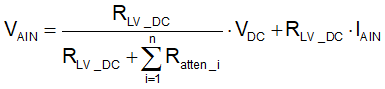
 Figure 8-16 DC-link Voltage Sensing Configuration