SLUSA87C August 2010 – October 2015 UCC24610
PRODUCTION DATA.
- 1 Features
- 2 Applications
- 3 Description
- 4 Revision History
- 5 Pin Configuration and Functions
- 6 Specifications
- 7 Detailed Description
-
8 Application and Implementation
- 8.1 Application Information
- 8.2
Typical Application
- 8.2.1 Design Requirements
- 8.2.2 Detailed Design Procedure
- 8.2.3 Application Curves
- 9 Power Supply Recommendations
- 10Layout
- 11Device and Documentation Support
- 12Mechanical, Packaging, and Orderable Information
Package Options
Mechanical Data (Package|Pins)
Thermal pad, mechanical data (Package|Pins)
- DRB|8
Orderable Information
8 Application and Implementation
NOTE
Information in the following applications sections is not part of the TI component specification, and TI does not warrant its accuracy or completeness. TI’s customers are responsible for determining suitability of components for their purposes. Customers should validate and test their design implementation to confirm system functionality.
8.1 Application Information
The UCC24610 synchronous rectifier controller is optimized for 5-V only applications, but may be used for other applications (such as LLC converters) where device stresses (such as VD voltage) are not exceeded, and a 5-V VCC source is available.
The effects of lead inductance on the VDS-sensing turnoff threshold varies with the SR MOSFET package. Compact packages such as SON, QFN, and similar packages have virtually no significant lead inductance in the drain connection, very little in the source, and nominal bond-wire inductance in the gate path. Slightly larger SOIC-derived packages may have 2-nH to 3-nH inductance in the source path. TO-220 and larger packages have significant lead inductances, which can adversely affect the turnoff point of the SR MOSFET unless the sensing is compensated for inductance. The falling dI/dt of the current through the SR lead inductance reduces the sensed VDS voltage and prematurely triggers turnoff. Resistors in the VD and VS sense paths can be used to compensate for this effect.
8.2 Typical Application
The following application information is applied to the UCC24610 Evaluation Module (EVM), which delivers 5 A at 5 V using an SR MOSFET in a TO-220 package. In this DCM flyback-topology application example, the SYNC signal is not used. Performance data relevant to the operation of the UCC24610 SR controller are included in this section for application reference. Refer to Using the UCC24610EVM-563 User's Guide (SLUU434) for additional details on the overall performance of the EVM. The schematic diagram for the EVM, Figure 22, is provided as an example of a typical application for the UCC24610.
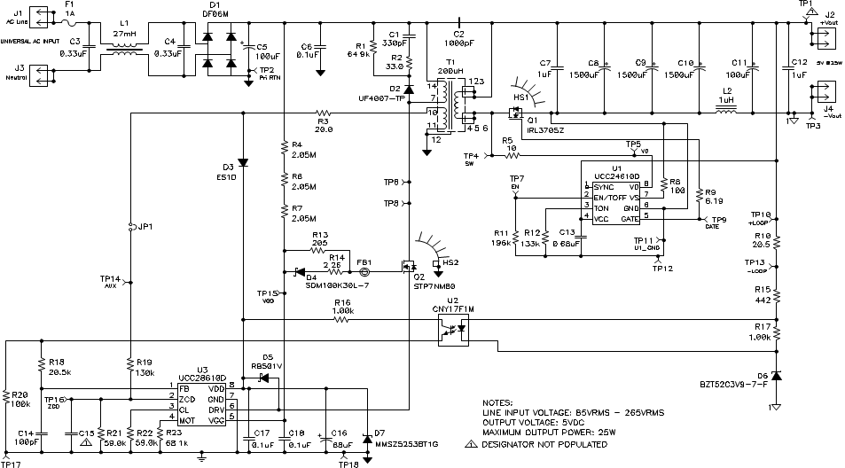 Figure 22. UCC24610 Typical Application Example
8.2.1 Design Requirements
Table 1. UCC24610 EVM Design Requirements
| PARAMETER | TEST CONDITIONS | MIN | NOM | MAX | UNIT | |
|---|---|---|---|---|---|---|
| INPUT CHARACTERISTICS | ||||||
| VIN | Input voltage | 85 | 265 | VRMS | ||
| IIN | Input current | VIN = 115 VRMS, IOUT = 5 A | 0.6 | ARMS | ||
| VIN = 115 VRMS, IOUT = 0 A | 0.03 | ARMS | ||||
| VUVLO | Brown out | IOUT = 5 A | 69 | VRMS | ||
| OUTPUT CHARACTERISTICS | ||||||
| VOUT | Output voltage, average | VIN = 85 VRMS to 265 VRMS, IOUT = 0 A to 5 A | 4.5 | 5 | 5.6 | V |
| VRIPPLE | Output voltage, ripple | VIN = 115 VRMS, IOUT = 5 A | 200 | mVpp | ||
| IOUT | Output current | VIN = 85 VRMS to 265 VRMS | 0 | 5 | A | |
| IOCP | Output overcurrent inception point | VIN = 115 VRMS | 7 | A | ||
| VOVP | Output overvoltage protection point | IOUT = 0 A to 5 A | 6.5 | V | ||
| Transient response voltage over-shoot | VIN = 115 VRMS, IOUT = 0 A to 5 A | 600 | mV | |||
| SYSTEM CHARACTERISTICS | ||||||
| fSW | Switching frequency | 26.3 | 140.4 | kHz | ||
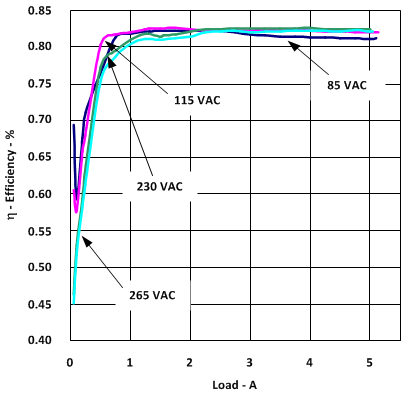
| ηPEAK | Peak efficiency | VIN = 115 VRMS, IOUT = 1.75 A | 82.7% | |||
| ηAVG | Average efficiency | VIN = 115 VRMS, IOUT = 25%, 50%, 75%, 100% of rated output current | 82.3% | |||
| VIN = 230 VRMS, IOUT = 25%, 50%, 75%, 100% of rated output current | 82.3% | |||||
| No-load power consumption | VIN = 115 VRMS, IOUT = 0 A | 181 | mW | |||
| VIN = 230 VRMS, IOUT = 0 A | 368 | mW | ||||
| Operating temperature range | VIN = 85 VRMS to 265 VRMS, IOUT = 0 A to 5 A | 25 | °C | |||
8.2.2 Detailed Design Procedure
8.2.2.1 VD and VS Detection
VD and VS are differential inputs used to sense the voltage across the SR-MOSFET to determine when to turn on and off the GATE output. When the GATE is off, the controller will not drive the GATE on until VD has exceeded 1.5 V at least once and TOFF has expired. Once these two conditions are met, the controller is armed to allow the GATE to turn on the next time the drain voltage falls 150 mV below the source voltage (VD – VS = –150 mV). While the GATE is off, the SR-MOSFET may be blocking reverse current, or forward current may be building up in the MOSFET body diode. Normally this body-diode current would generate about 700 mV forward voltage drop (–700 mVDS), but when –150 mV is detected the GATE is turned on to enhance the MOSFET into a synchronous rectifier. The GATE stays on for at least the minimum on time TON or longer until the SR-MOSFET current diminishes to near zero. When the current reduces sufficiently such that the VDS voltage drop is only
–5 mV, the GATE output is turned off. (It can be seen that the MOSFET RDS(on) determines the current level at which the GATE is turned off, which then further factors into determining the light-load mode inception point.) At the same time, the controller is disarmed to prevent spurious GATE output. Because the MOSFET current is not yet zero at GATE turn off, the VDS will briefly increase back up to the body-diode drop, however the additional power loss is very small. The disarmed state of the controller prevents repeated turn on of the GATE (even though VDS ≤150 mV again). Once the current does decrease to zero, the drain voltage climbs past the 1.5-V threshold, at which point the minimum off-time interval TOFF is triggered. Once VDS has exceeded 1.5 V and TOFF has expired, the GATE circuit is rearmed to respond to the next turnon condition.
Because the VD and VS inputs are connected across the SR-MOSFET body diode by way of its package leads, the high secondary-side dI/dt through the lead inductances can impress excessive negative voltage on the VD pin. This negative voltage can disrupt normal controller operation and prevent the device from switching. This problem can be avoided by limiting the current drawn out of the VD pin to less than 100 mA. A resistor placed in series between VD and the SR-MOSFET drain can be sized to provide the proper current limiting.
This resistor value is calculated by Equation 1.

where
- LPKG is the total package inductance between the drain and source pads of the SR-MOSFET when mounted on the PCB,
- dISEC/dt is the rate of rise of the secondary current after the primary-side switch turns off.
Include any stray trace inductance if the device GND pin is not connected directly to the SR-MOSFET source pad.
The bias current of the VD pin through RVD (if any) generates a small offset voltage that can cause an apparent shift in the SR-MOSFET turnoff threshold, leading to earlier turn off than desired, depending on the value of RVD. To counter this offset voltage, a resistor of equal value can be placed in series with the VS pin to balance the VD–VS comparator inputs (RVS = RVD).
Larger MOSFET packages such as TO-220 and TO-247 generally have significant internal inductances (on the order of 10 nH ≈ 20 nH), and are used in higher-power applications where dI/dt can be quite high. On the other hand, low-power applications using smaller packages such as QFN style and even DPAK style or equivalent MOSFETs can have a sufficiently low L × dI/dt product such that RVD and RVS may not be necessary. Refer to the MOSFET datasheet or consult with the manufacturer to determine the total inductance for the specific MOSFET being considered for a synchronous-rectifier application.
8.2.2.2 Enabling and TOFF Programming
The controller must be out of UVLO mode, or the internal current source on EN/TOFF pin is shut off and the pin is pulled low with an internal 10-kΩ resistor. Before the device is in the Enabled state, the current source on EN/TOFF delivers 20 μA. Prudent design practice indicates that a minimum REN/TOFF value of 93 kΩ is necessary to ensure the pin voltage exceeds the disable threshold. After being Enabled, the Enabled state is latched and the source current reduces to 10 μA. This current level establishes the voltage that determines the TOFF time, as shown in Equation 2 through Equation 5.
When both the VCC and EN/TOFF conditions are met to enable the device, an internal power-up sequence ensures that the controller starts the SR-MOSFET synchronously with the system conduction conditions. This avoids turnon of the SR-MOSFET into an inappropriate system state. After a ≈25-μs delay to allow internal references to stabilize, SR operation commences in light-load mode and the load condition is monitored at the first complete switching cycle after the delay to determine the next operating mode.
Because VDS of the SR-MOSFET may ring above 1.5 V and back below –150 mV one or more times (due to circuit parasitic elements), TOFF time should be programmed to block GATE re-arming for the duration of this ringing. In a system, the duration of this ringing may be unknown until actual prototypes are operational and observable, so a longer TOFF time may be initially programmed and the final value adjusted after system evaluation and optimization.
Nominal TOFF off time is programmed by Equation 2 through Equation 5, where TOFF is in μs and REN/TOFF is in MΩ.

valid for:

Conversely,

valid for:

For any REN/TOFF > 282 kΩ, TOFF = 0.65 μs.
For any 70 kΩ < REN/TOFF < 80 kΩ, VEN toggles rapidly between 1.4 V and 0.8 V and the device remains disabled. In this situation, average ICC is approximately half of the normal run-mode current, ICC(on).
For any REN/TOFF < 70 kΩ, VEN is < 1.4 V and the device is disabled, operating in sleep mode.
8.2.2.3 TON Programming
The voltage on this pin is internally regulated to 2 V, and an external resistor to GND sets a current which programs the minimum on time TON. If a noise-filter capacitor is deemed to be necessary on this pin, do not exceed 100 pF to avoid instability of the 2-V regulator.
Because VDS of the SR-MOSFET may ring above –5 mV one or more times immediately after turn on (due to circuit parasitic elements) TON time should be programmed to block GATE turn off for the duration of this spurious ringing. In a system, the duration of this ringing may be unknown until actual prototypes are operational and observable, so a longer TON time may be initially programmed and the final value adjusted after system evaluation and optimization.
Nominal TON minimum on time is programmed by Equation 6 through Equation 9, where TON is in µs and RTON is in MΩ.

Valid for:

Conversely,

Valid for:

For resistance values of RTON outside of the previous range given, the device may enter a fault-protection mode as described in Fault Mode and Other Protections.
8.2.2.4 GATE Drive and RGATE Considerations
The GATE output driver is capable of sourcing >1-A peak current into the SR-MOSFET gate, and sinking >2 A out of it. Standard low-inductance, low-loop-area design techniques should be employed to minimize stray inductance, which slows the MOSFET turn on and increases gate-drive ringing.
A series resistance RGATE from the GATE output to the MOSFET gate is used to damp this ringing, and its value is chosen based on the standard critical damping formula for a series-LCR resonant tank, see Equation 10.

where
- Lg is the total series gate-loop inductance,
- Ciss is the total effective input capacitance of the MOSFET,
- rg is the internal gate resistance of the MOSFET.
NOTE
The total series resistance in the gate-drive path may also limit the peak GATE currents obtainable below the rated capabilities of the device’s GATE output driver stage.
8.2.2.5 VCC Range and Bypassing Considerations
With a normal operating range of 4.5 V to 5.5 V, the device is well suited for 5-V nominal output applications and can easily accommodate ±10% transient VCC excursions due to system line and load disturbances. When the average VCC voltage approaches the VCC(off) threshold (UVLO), system ripple and noise on VCC may cross that threshold and shut down the controller unless adequate decoupling is provided from VCC to GND at the controller pins.
High peak gate-drive currents during the GATE turnon transition also require sufficient local capacitive bypassing of the VCC pin to GND. For smaller SR-MOSFETs a minimum value of 0.1 μF may be sufficient, but larger MOSFETs may require additional bypass capacitance to avoid excess ripple on the VCC voltage.
Suggested VCC bypass capacitance is 0.1 μF for each 2.2 nF of Ciss.
8.2.2.6 SYNC Input Considerations
In applications where the synchronous rectifier is used in continuous conduction mode (CCM) such as CCM-Flyback and LLC converters, it is imperative that the SR-MOSFET be turned off as soon as the primary-side switch turns on, to prevent reverse conduction of the SR-MOSFET. In these applications, a Y-type isolating capacitor CSYNC can be used to convey a primary-side signal to the SR controller by coupling a negative-going trigger voltage into the SYNC pin. Alternatively, an isolating pulse transformer may be used in situations where a coupling capacitor is not practicable. When the SYNC voltage falls 2 V below VCC (the SYNC detection threshold VTHSYNC), the GATE output is immediately turned off, regardless of the state of the TON timer. An internal 2-kΩ pullup resistance (rSYNC) provides current to recharge the SYNC coupling capacitor. In the event that the SYNC input voltage is continuously held below VTHSYNC, the GATE output is driven low for the same duration.
The SYNC input has a maximum pulse current rating of ±100 mA, and a high-reliability design should reduce the peak current further. This also reduces noise and signal losses in the system. A series resistor helps limit the pulse current by reducing the effective dV/dt across CSYNC. Figure 23 illustrates a simple implementation of the SYNC signal derived from the falling drain-source voltage of the primary-side MOSFET. In this example, a synchronous-rectifier MOSFET is used in place of the free-wheeling diode in a single-transistor forward-mode application. Note that primary-to-secondary common-mode capacitance CCM forms the return path for the SYNC current.
Nominally, only –1 mA is required to develop –2 V across the internal 2-kΩ resistance and trigger the SYNC function. This current is generated by a rapidly changing voltage across the SYNC coupling capacitor CSYNC. But variations of this resistor, of CSYNC, and of the dV/dt across CSYNC require that worst-case tolerances be taken into account when determining the minimum value of CSYNC. In addition, VSYNC must exceed the VTHSYNC threshold for a minimum duration of 20 ns to ensure that the internal controller logic has reliably triggered.
Although the TON minimum on-time gate-drive function is overridden by the SYNC signal, the timer continues to function otherwise. Light-load mode is entered if the proper conditions are met, as usual. The TOFF timer is triggered when the SR-MOSFET VDS exceeds 1.5 V, as usual.
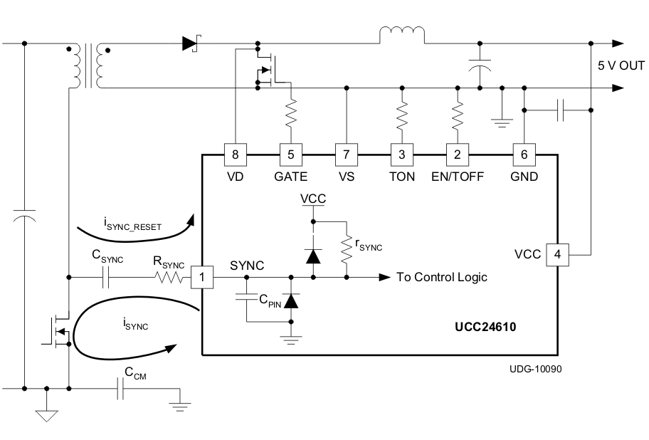 Figure 23. Driving the SYNC Input from the Primary-Side MOSFET Drain
CSYNC is the synchronization signal coupling capacitor, rated to cross the primary-to-secondary isolation boundary. It is used to couple a negative-going voltage into the UCC24610 SYNC input (pin 1) to turn off the GATE output to the SR-MOSFET when the primary-side MOSFET is turned on.
RSYNC is an optional external current-limiting resistor used to reduce the peak current into the SYNC input. It also serves to reduce overall power loss, and reduce the common-mode noise current.
CCM is the main common-mode capacitance between the primary and the secondary sides of the system. This is usually a discrete component, whose value ranges from 100 pF ≈2200 pF. Aside from any EMI-control purposes, it also serves as the return path for the SYNC signal charging and discharging current pulses across the isolation boundary.
Within the UCC24610 controller device is a 2-kΩ pullup resistor (rSYNC) to VCC. To trigger the SYNC function, a negative-going signal must pull the SYNC input below the VTHSYNC threshold (nominally 2 V below VCC) for a minimum duration of 20 ns. This requires a minimum 1-mA current to achieve, but prudent design will target a higher current to allow for parameter variations.
Internal clamp diodes to VCC and GND also form parts of the charging and discharging current paths of the SYNC signal. Finally, CPIN comprises stray internal and external pin and pad capacitances on the SYNC input, and is modeled as ≈10 pF to GND. Although CPIN is physically unavoidable, it is wise to minimize any external stray capacitance to keep its effect of additional delay on the SYNC function to a minimum.
8.2.2.6.1 Determine the Minimum Change
Determine the minimum change in voltage ΔVSYNC-pri expected from the SYNC signal source. In this example, the primary-side MOSFET drain-to-source voltage VDS_PRI is the signal source, and its minimum change is VBULK(min) at low input line.
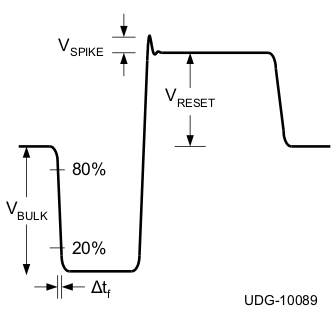
| ΔVDS_PRI = VBULK at low-line | Δtf = fall time for ΔVDS_PRI
between the 80% and 20% points |
VSYNC-pri = ΔVDS_PRI |
To allow for parameter and environmental variations, set the minimum peak SYNC current to 2 mA. With 2-mA peak flowing through the internal 2-kΩ resistor, the SYNC voltage falls to 4-V below VCC. The maximum value for current limiting resistor RSYNC is determined by Equation 11 and Equation 12.

so in this case,

8.2.2.6.2 After the ΔVDS_PRI Transition
After the ΔVDS_PRI transition, the SYNC signal will begin to reset back to VCC by charging exponentially. This allows the value of the SYNC coupling capacitor CSYNC to be determined by Equation 13.

The value of CSYNC is chosen to ensure that the SYNC signal stays below the SYNC threshold for at least 20 ns. Choose the minimum dwell time tMIN to be 40 ns to allow for parametric variations, shown in Equation 14.

8.2.2.6.3 The Value of CCM
The value of CCM should be much higher than that of CSYNC. If necessary, increase the value of CCM to ensure that CCM >> CSYNC; do not decrease CSYNC.
8.2.2.6.4 Conservative Power-Loss Estimates
Conservative power-loss estimates for the internal and external SYNC resistances are:

and

where
- fSW is the converter switching frequency.
These calculations can be used to predict the maximum thermal impact of the SYNC current on the device junction temperature and to determine the external SYNC resistor power rating. Actual SYNC-related losses generally are lower than these calculations predict and observations of actual circuit operation should be used to determine true losses if more accuracy is required.
8.2.2.6.5 The Device Internal SYNC-to-GATE Delay Time
The device internal SYNC-to-GATE delay time tSDLY is a measure of how quickly the GATE output will turn off after the SYNC signal has crossed the VTHSYNC threshold. However, stray pin capacitance CPIN introduces an additional delay to the SYNC function by slowing the SYNC voltage falling 2-V below VCC. If CPIN is small, this delay is relatively short and the SYNC current can be approximated as a constant current, allowing this calculation to simplify to a simple linear equation given by:

Also, additional delay comes from the finite dV/dt of the signal source, in this case VDS_PRI, due to the finite transition time from VBULK level to 0 V. This delay can be approximated by:

These delay times should be added to the internal SYNC-to-GATE delay to determine the total delay time expected between the falling of the primary-side MOSFET drain voltage and the turn off of the SR-FET gate drive.

8.2.2.6.6 The CSYNC Capacitor Resets
The CSYNC capacitor resets during the off-time of the primary-side MOSFET, while the SR-FET is conducting. The reset current iSYNC_RESET is similar to iSYNC. However, this reset current flows through the internal diode between SYNC and VCC pins of the device.
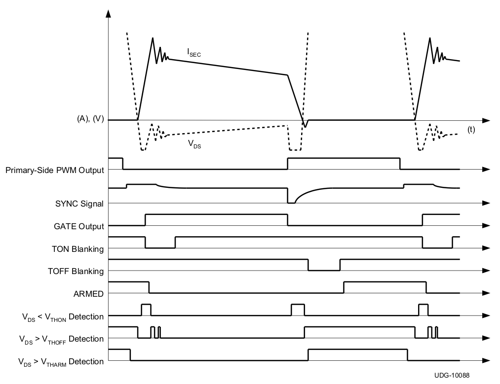 Figure 25. External and Internal Signal Timing Relationships with Respect to Realistic CCM Waveforms
8.2.2.7 Single-Fault Self-Protection Features
If RTON is less than 8.7 kΩ, the device may detect excess current and interpret this as a short-cir cuit and disable the GATE output.
If RTON is greater than 301 kΩ, the device may detect insufficient current and interpret this as an open-circuit and disable the GATE output, to avoid indefinite on-time.
Noise pick-up on excessive trace length may destabilize the internal 2-V source causing either insufficient or excess current to RTON and triggering premature GATE shut off. This could cause GATE output to be less than TON and lead to light-load mode even at heavy loads. Minimize RTON trace lengths.
If REN/TOFF is less than 93 kΩ, the device may detect insufficient voltage for Enable threshold and disable the GATE output.
If REN/TOFF is greater than 284 kΩ, the device will internally clamp the programming voltage to deliver a minimum TOFF of ≈0.65 µs, regardless of REN/TOFF value.
8.2.3 Application Curves
The following oscilloscope screen-captures and performance data illustrate the operation of the UCC24610 SR controller as applied in the UCC24610EVM-563 evaluation module, using, in part, the design method and equations found in Detailed Design Procedure. These select figures are reproduced from Using the UCC24610EVM-563 User's Guide (SLUU434).
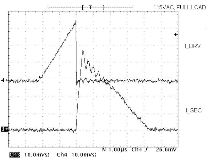
| 115-VAC input | 5-A load |
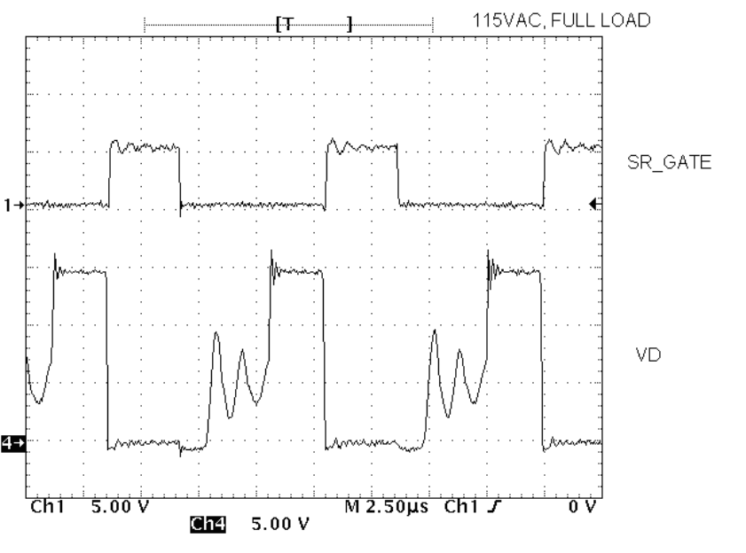
| 115-VAC input | 5-A load |
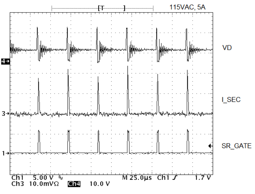
| 115-VAC input | 5-A load |
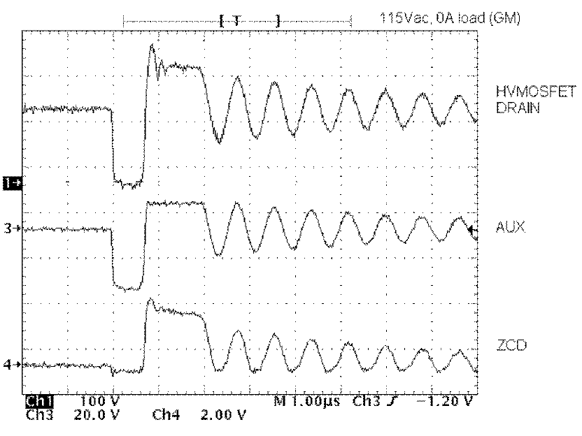
| 115-VAC Input | 0-A load | green mode |
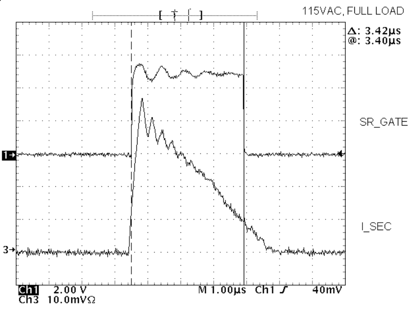
| 115-VAC input | 5-A load |

| 115-VAC input | 5-A load |
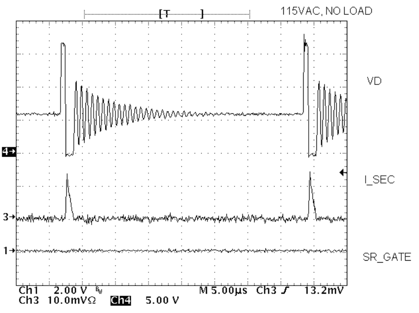
| 115-VAC Input | 0-A load | green mode |
