SLUSA87C August 2010 – October 2015 UCC24610
PRODUCTION DATA.
- 1 Features
- 2 Applications
- 3 Description
- 4 Revision History
- 5 Pin Configuration and Functions
- 6 Specifications
- 7 Detailed Description
-
8 Application and Implementation
- 8.1 Application Information
- 8.2
Typical Application
- 8.2.1 Design Requirements
- 8.2.2 Detailed Design Procedure
- 8.2.3 Application Curves
- 9 Power Supply Recommendations
- 10Layout
- 11Device and Documentation Support
- 12Mechanical, Packaging, and Orderable Information
Package Options
Mechanical Data (Package|Pins)
Thermal pad, mechanical data (Package|Pins)
- DRB|8
Orderable Information
10 Layout
10.1 Layout Guidelines
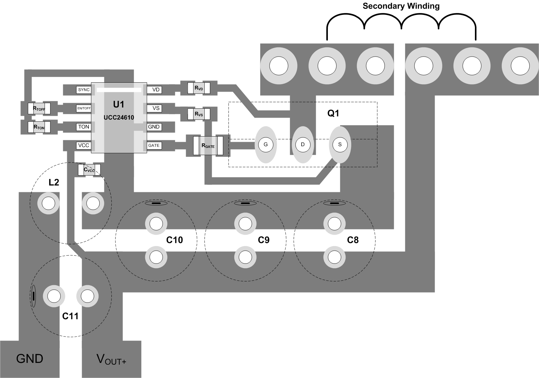
The printed circuit board (PCB) requires conscientious layout to minimize current loop areas and track lengths, especially when using single-sided PCBs.
- Place a ceramic MLCC bypass capacitor as close as possible to VCC and GND.
- Avoid connecting VD and VS sense points at locations where stray inductance is added to the SR MOSFET package inductance, as this will tend to turn off the SR prematurely.
- Run a track from the VD pin directly to the MOSFET drain pad to avoid sensing voltage across the stray inductance in the SR drain current path. Include an RVD component option in series with the VD pin unless previous testing has shown that it is not necessary.
- Run a track from the VS pin directly to the MOSFET source pad to avoid sensing voltage across the stray inductance in the SR source current path. Do not simply connect VS to the controller GND pin. Include an RVS component option in series with the VS pin unless previous testing has shown that it is not necessary.
- Run parallel tracks from GATE and GND to the SR MOSFET. Include a series gate resistance to dampen ringing.
10.2 Layout Example
 Figure 34. Single-Sided PCB Layout Using a TO-220 MOSFET