SLUSA87C August 2010 – October 2015 UCC24610
PRODUCTION DATA.
- 1 Features
- 2 Applications
- 3 Description
- 4 Revision History
- 5 Pin Configuration and Functions
- 6 Specifications
- 7 Detailed Description
-
8 Application and Implementation
- 8.1 Application Information
- 8.2
Typical Application
- 8.2.1 Design Requirements
- 8.2.2 Detailed Design Procedure
- 8.2.3 Application Curves
- 9 Power Supply Recommendations
- 10Layout
- 11Device and Documentation Support
- 12Mechanical, Packaging, and Orderable Information
Package Options
Mechanical Data (Package|Pins)
Thermal pad, mechanical data (Package|Pins)
- DRB|8
Orderable Information
5 Pin Configuration and Functions
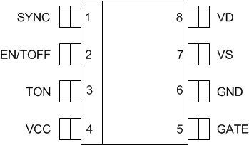
D Package
8-Pin SOIC
Top View

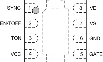
DRB Package
8-Pin SON With Exposed Thermal Pad
Top View

Pin Functions
| PIN | I/O | DESCRIPTION | |
|---|---|---|---|
| NAME | NO. | ||
| EN/TOFF | 2 | I |
EN/TOFF (combined enable function and programmable off-time timer), when VCC falls below the VCC(off) threshold, the UCC24610 is in UVLO mode, the EN/TOFF input is internally connected to GND through a 10-kΩ resistance and the internal current source is turned off. When VCC exceeds the VCC(on) threshold, the 10-kΩ resistance is removed and the current source is turned on. Thereafter, when EN/TOFF exceeds VEN(on), the UCC24610 is in run mode and when EN/TOFF falls below VEN(off), the UCC24610 is in sleep mode. The voltage level on EN/TOFF also programs the minimum off-time (TOFF) for the controlled MOSFET. EN/TOFF is internally driven by a two-level current source, so the voltage level on EN/TOFF can be set by connecting a resistor from EN/TOFF to GND. The EN/TOFF current source initially drives twice as much current (IEN-START) to achieve the enable threshold voltage VEN(on), and then drops to the normal run mode level (IEN-ON) to program the TOFF time. Alternatively, the desired EN/TOFF voltage may be forced using an external source. The TOFF time is programmed to suppress GATE output for a desired duration to avoid possible false retriggering from resonant ringing or noise after turnoff. The TOFF timer is triggered when VD voltage exceeds 1.5 V after GATE transitions from high to low. |
| GATE | 5 | O |
GATE (controlled MOSFET gate drive), connect GATE to the gate of the controlled MOSFET through a small series resistor using short PC board tracks to achieve optimal switching performance. The GATE output can achieve >1-A peak source current when High and >2-A peak sink current when Low into a large N-channel power MOSFET. In sleep mode and UVLO, GATE impedance to GND is about 1.6 Ω. GATE impedance to GND crests about 80 Ω, when VCC ≈ 1.1 V. |
| GND | 6 | – |
GND (combined analog and power ground), this ground input is the reference potential for the GATE driver, the UVLO comparator, the EN/TOFF comparator, the EN/TOFF timer, and the TON timer. Connect a 0.1-µF or larger ceramic bypass capacitor from the VCC pin to the GND pin through very short PC-board tracks. |
| SYNC | 1 | I |
SYNC (gate turnoff synchronization), a falling edge on SYNC immediately forces GATE low, turning off the controlled MOSFET asynchronous to the voltage on the drain and source, and regardless of the state of the TON timer. When a power converter is operated in continuous conduction mode (CCM), it is necessary to turn off the controlled MOSFET under command of the switching converter. Connect SYNC to a control signal on the primary side of the converter using a high-voltage isolation capacitor or transformer, or other suitable coupling means. A continuous low level on the SYNC input causes GATE to be driven low for the same duration. |
| TON | 3 | I |
TON (programmable on-time timer), program the minimum on time with a resistor from TON to GND. When the controlled MOSFET gate is turned on, some ringing noise is generated. The minimum on-time timer blanks the VD-VS comparator, keeping the controlled MOSFET on for at least the programmed minimum time. This time also determines the light-load shut-down point. If VD-VS falls below the –5-mV threshold before TON time expires, the controller transitions into light-load mode on the next switching cycle. When VD-VS falls below the –5-mV threshold after TON expires, the device resumes run-mode operation on the next switching cycle. |
| VCC | 4 | I |
VCC (positive power input), connect a DC power voltage to VCC. Bypass VCC to GND with a 0.1-µF or larger ceramic capacitor using short PC board tracks. VCC supplies power to all circuits in the UCC24610. Under-Voltage Lockout (UVLO) comparators prevent operation until VCC rises above VCC(on). VCC can be used to safely turn off the UCC24610 by pulling VCC below VCC(off). In the event that VCC drops below VCC(off), GATE immediately falls Low and EN/TOFF is internally connected to GND with a 10-kΩ resistance. |
| VD | 8 | I |
VD (drain-sense voltage), connect this pin as close as possible to the controlled MOSFET drain pad through a short PC board track, to minimize the effects of trace inductance on VD. VD must be >1.5 V and the TOFF timer must be expired before the device may be armed to allow the controlled MOSFET to be turned on the next switching cycle. Once armed, the controlled MOSFET is turned on (GATE goes High) when VD falls more than –150 mV below VS. At that threshold, the GATE output goes High and the TON timer is triggered. GATE remains High at least as long as the programmed TON time has not expired, unless a pulse at the SYNC input is detected. After TON has expired, the GATE output is turned off when VD-VS voltage decreases to –5 mV. If VD-VS decreases to –5 mV before TON expires, the controller enters light-load mode and the GATE pulse for the next switching cycle is suppressed. When the VD voltage increases to 1.5 V, the TOFF timer is triggered and the GATE output is prevented from turning on during the TOFF interval. |
| VS | 7 | I |
VS (source-sense voltage), connect this pin as close as possible to the controlled MOSFET source pad through a short PC-board track, to minimize the effects of trace inductance on VS. |
| Thermal Pad | – |
Thermal Pad on SON package only, the exposed thermal pad on the bottom of the SON package enhances the thermal performance of the device, and is intended to be soldered to a heat-dissipating pad on the PCB. This pad should be connected to the GND pin, or may be left floating (unconnected to any network). It is internally connected to GND through an indeterminate impedance and so may not be used to carry current. |
|