SLUS504I September   2002  – November 2023 UCC27321 , UCC27322 , UCC37321 , UCC37322

PRODUCTION DATA  

  1.   1
  2. Features
  3. Applications
  4. Description
  5. Description (continued)
  6. Related Products
  7. Pin Configuration and Functions
  8. Specifications
    1. 7.1 Absolute Maximum Ratings
    2. 7.2 ESD Ratings
    3. 7.3 Recommended Operating Conditions
    4. 7.4 Thermal Information
    5. 7.5 Electrical Characteristics
    6. 7.6 Switching Characteristics
    7. 7.7 Power Dissipation Ratings
    8. 7.8 Typical Characteristics
  9. Detailed Description
    1. 8.1 Overview
    2. 8.2 Functional Block Diagram
    3. 8.3 Feature Description
      1. 8.3.1 Input Stage
      2. 8.3.2 Output Stage
      3. 8.3.3 Source and Sink Capabilities during Miller Plateau
      4. 8.3.4 Enable
    4. 8.4 Device Functional Modes
  10. Application and Implementation
    1. 9.1 Application Information
    2. 9.2 Typical Application
      1. 9.2.1 Design Requirements
      2. 9.2.2 Detailed Design Procedure
        1. 9.2.2.1 Input-to-Output Configuration
        2. 9.2.2.2 Input Threshold Type
        3. 9.2.2.3 VDD Bias Supply Voltage
        4. 9.2.2.4 Peak Source and Sink Currents
        5. 9.2.2.5 Enable and Disable Function
        6. 9.2.2.6 Propagation Delay
        7. 9.2.2.7 Power Dissipation
      3. 9.2.3 Application Curves
  11. 10Power Supply Recommendations
    1.     40
  12. 11Layout
    1. 11.1 Layout Guidelines
    2. 11.2 Layout Example
    3. 11.3 Thermal Considerations
  13. 12Device and Documentation Support
    1. 12.1 Device Support
      1. 12.1.1 Third-Party Products Disclaimer
    2. 12.2 Documentation Support
      1. 12.2.1 Related Documentation
    3. 12.3 Receiving Notification of Documentation Updates
    4. 12.4 Support Resources
    5. 12.5 Trademarks
    6. 12.6 Electrostatic Discharge Caution
    7. 12.7 Glossary
  14. 13Revision History
  15. 14Mechanical, Packaging, and Orderable Information

Package Options

Refer to the PDF data sheet for device specific package drawings

Mechanical Data (Package|Pins)
  • D|8
  • P|8
  • DGN|8
Thermal pad, mechanical data (Package|Pins)
Orderable Information

Description

The UCC2732x/UCC3732x family of high-speed drivers deliver 9 A of peak drive current in an industry standard pinout. These drivers can drive the largest of MOSFETs for systems requiring extreme Miller current due to high dV/dt transitions. This eliminates additional external circuits and can replace multiple components to reduce space, design complexity, and assembly cost. Two standard logic options are offered, inverting (UCC37321) and noninverting (UCC37322).

Device Information
PART NUMBERPACKAGE(1)BODY SIZE (NOM)
UCC2732x
UCC3732x
MSOP-PowerPAD (8)3.00 mm × 3.00 mm
SOIC (8)3.91 mm × 4.90 mm
For all available packages, see the orderable addendum at the end of the data sheet.
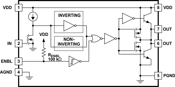
GUID-E59678EA-B6DE-4F78-B327-D00D9DBE4479-low.gif Block Diagram