SLUSBA7G December   2012  – June 2019 UCC27531 , UCC27533 , UCC27536 , UCC27537 , UCC27538

PRODUCTION DATA.  

  1. Features
  2. Applications
  3. Description
    1.     Device Images
      1.      Driving IGBT Without Negative Bias
  4. Revision History
    1.     Description (continued)
  5. Device Comparison Table
  6. Pin Configuration and Functions
    1.     Pin Functions
  7. Specifications
    1. 7.1 Absolute Maximum Ratings
    2. 7.2 ESD Ratings
    3. 7.3 Recommended Operating Conditions
    4. 7.4 Thermal Information
    5. 7.5 Electrical Characteristics
    6. 7.6 Switching Characteristics
    7. 7.7 Timing Diagrams
    8. 7.8 Typical Characteristics
  8. Detailed Description
    1. 8.1 Overview
    2. 8.2 Functional Block Diagrams
    3. 8.3 Feature Description
      1. 8.3.1 VDD Undervoltage Lockout
      2. 8.3.2 Input Stage
      3. 8.3.3 Enable Function
      4. 8.3.4 Output Stage
    4. 8.4 Device Functional Modes
  9. Applications and Implementation
    1. 9.1 Application Information
    2. 9.2 Typical Application
      1. 9.2.1 Driving IGBT Without Negative Bias
        1. 9.2.1.1 Design Requirements
        2. 9.2.1.2 Detailed Design Procedure
          1. 9.2.1.2.1 Input-to-Output Configuration
          2. 9.2.1.2.2 Input Threshold Type
          3. 9.2.1.2.3 VDD Bias Supply Voltage
          4. 9.2.1.2.4 Peak Source and Sink Currents
          5. 9.2.1.2.5 Enable and Disable Function
          6. 9.2.1.2.6 Propagation Delay
          7. 9.2.1.2.7 Power Dissipation
        3. 9.2.1.3 Application Curve
      2. 9.2.2 Driving IGBT With 13-V Negative Turn-Off BIAS
        1. 9.2.2.1 Design Requirements
        2. 9.2.2.2 Detailed Design Procedure
        3. 9.2.2.3 Application Curve
      3. 9.2.3 Single-Output Driver
        1. 9.2.3.1 Design Requirements
        2. 9.2.3.2 Detailed Design Procedure
        3. 9.2.3.3 Application Curve
      4. 9.2.4 Using UCC2753x Drivers in an Inverter
        1. 9.2.4.1 Design Requirements
        2. 9.2.4.2 Detailed Design Procedure
        3. 9.2.4.3 Application Curve
  10. 10Power Supply Recommendations
  11. 11Layout
    1. 11.1 Layout Guidelines
    2. 11.2 Layout Example
    3. 11.3 Thermal Consideration
  12. 12Device and Documentation Support
    1. 12.1 Related Links
    2. 12.2 Trademarks
    3. 12.3 Electrostatic Discharge Caution
    4. 12.4 Glossary
  13. 13Mechanical, Packaging, and Orderable Information

Package Options

Mechanical Data (Package|Pins)
Thermal pad, mechanical data (Package|Pins)
Orderable Information

Application Curve

The following application curves were observed using the UCC27531 on the UCC27531EVM-184.

NOTE

Legend: Green: EVM PWM Input, Blue: UCC27531 IN, Red: EVM GATE Output

UCC27531 UCC27533 UCC27536 UCC27537 UCC27538 fig6_luua70.gifFigure 42. UCC27531DBV Input vs. Output PWM Propagation Delay (High)
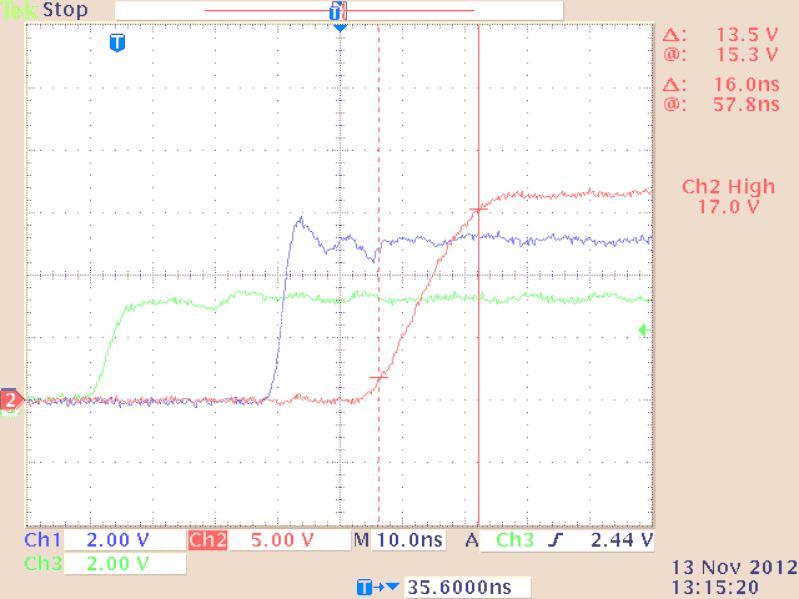
UCC27531 UCC27533 UCC27536 UCC27537 UCC27538 fig8_luua70.gifFigure 44. UCC27531DBV Input vs. Output PWM Rise Time
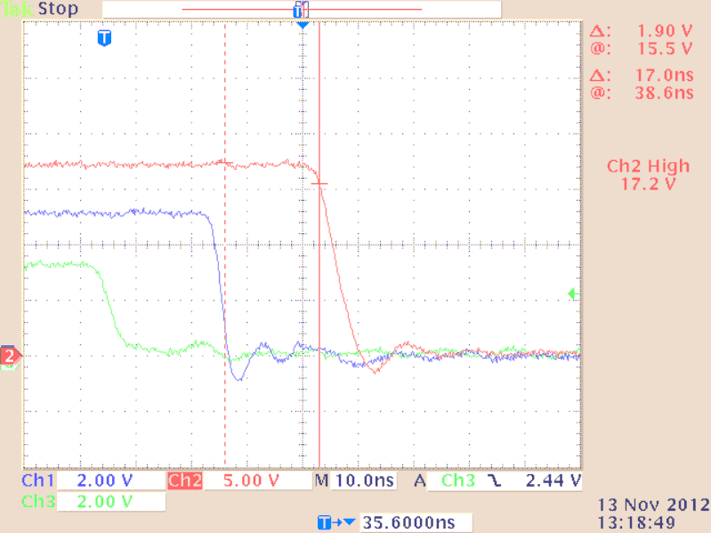
UCC27531 UCC27533 UCC27536 UCC27537 UCC27538 fig7_luua70.gifFigure 43. UCC27531DBV Input vs. Output PWM Propagation Delay (Low)