SLUSBA7G December   2012  – June 2019 UCC27531 , UCC27533 , UCC27536 , UCC27537 , UCC27538

PRODUCTION DATA.  

  1. Features
  2. Applications
  3. Description
    1.     Device Images
      1.      Driving IGBT Without Negative Bias
  4. Revision History
    1.     Description (continued)
  5. Device Comparison Table
  6. Pin Configuration and Functions
    1.     Pin Functions
  7. Specifications
    1. 7.1 Absolute Maximum Ratings
    2. 7.2 ESD Ratings
    3. 7.3 Recommended Operating Conditions
    4. 7.4 Thermal Information
    5. 7.5 Electrical Characteristics
    6. 7.6 Switching Characteristics
    7. 7.7 Timing Diagrams
    8. 7.8 Typical Characteristics
  8. Detailed Description
    1. 8.1 Overview
    2. 8.2 Functional Block Diagrams
    3. 8.3 Feature Description
      1. 8.3.1 VDD Undervoltage Lockout
      2. 8.3.2 Input Stage
      3. 8.3.3 Enable Function
      4. 8.3.4 Output Stage
    4. 8.4 Device Functional Modes
  9. Applications and Implementation
    1. 9.1 Application Information
    2. 9.2 Typical Application
      1. 9.2.1 Driving IGBT Without Negative Bias
        1. 9.2.1.1 Design Requirements
        2. 9.2.1.2 Detailed Design Procedure
          1. 9.2.1.2.1 Input-to-Output Configuration
          2. 9.2.1.2.2 Input Threshold Type
          3. 9.2.1.2.3 VDD Bias Supply Voltage
          4. 9.2.1.2.4 Peak Source and Sink Currents
          5. 9.2.1.2.5 Enable and Disable Function
          6. 9.2.1.2.6 Propagation Delay
          7. 9.2.1.2.7 Power Dissipation
        3. 9.2.1.3 Application Curve
      2. 9.2.2 Driving IGBT With 13-V Negative Turn-Off BIAS
        1. 9.2.2.1 Design Requirements
        2. 9.2.2.2 Detailed Design Procedure
        3. 9.2.2.3 Application Curve
      3. 9.2.3 Single-Output Driver
        1. 9.2.3.1 Design Requirements
        2. 9.2.3.2 Detailed Design Procedure
        3. 9.2.3.3 Application Curve
      4. 9.2.4 Using UCC2753x Drivers in an Inverter
        1. 9.2.4.1 Design Requirements
        2. 9.2.4.2 Detailed Design Procedure
        3. 9.2.4.3 Application Curve
  10. 10Power Supply Recommendations
  11. 11Layout
    1. 11.1 Layout Guidelines
    2. 11.2 Layout Example
    3. 11.3 Thermal Consideration
  12. 12Device and Documentation Support
    1. 12.1 Related Links
    2. 12.2 Trademarks
    3. 12.3 Electrostatic Discharge Caution
    4. 12.4 Glossary
  13. 13Mechanical, Packaging, and Orderable Information

Package Options

Mechanical Data (Package|Pins)
Thermal pad, mechanical data (Package|Pins)
Orderable Information

Pin Configuration and Functions

5-Pin or 6-Pin SOT-23
DBV Package
Top View
UCC27531 UCC27533 UCC27536 UCC27537 UCC27538 pin_lusba7.gif
8-Pin SOIC
D Package
Top View
UCC27531 UCC27533 UCC27536 UCC27537 UCC27538 8pins.gif

Pin Functions

PIN I/O DESCRIPTION
NAME NO.
UCC27531DBV
1 EN I Enable (Pull EN to GND to disable output, pull it high or leave open to enable output)
2 IN I Driver non-inverting input
3 VDD I Bias supply input
4 GND - Ground (all signals are referenced to this node)
5 OUTL O 5-A sink current output of driver
6 OUTH O 2.5-A Source Current Output of driver
UCC27533DBV
1 VDD I Bias supply input
2 GND - Ground (All signals are referenced to this node)
3 IN+ I Driver non-inverting input
4 IN- I Driver inverting input
5 OUT O 2.5-A source and 5-A sink current output of driver
UCC27536DBV
1 EN I Enable (pull EN to GND to disable output, pull it high or leave open to enable output)
2 GND - Ground (all signals are referenced to this node)
3 IN- I Driver inverting input
4 OUT O 2.5-A source and 2.5-A sink current output of driver
5 VDD I Bias supply input
UCC27537DBV
1 EN I Enable (Pull EN to GND to disable Output, Pull it high or leave open to enable Output)
2 GND - Ground (All signals are referenced to this node)
3 IN+ I Driver non-inverting input
4 OUT O 2.5-A source and 5-A sink current output of driver
5 VDD I Bias supply input
UCC27538DBV
1 VDD I Bias supply input
2 IN1 I Driver non-inverting input
3 GND - Ground (all signals are referenced to this node)
4 OUTL O 5-A sink current output of driver
5 IN2 I Driver non-inverting input
6 OUTH O 2.5-A source current output of driver
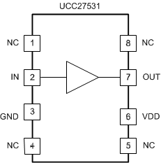
UCC27531D
1 NC - No connection
2 IN I Driver non-inverting input
3 GND - Ground (all signals are referenced to this node)
4 NC - No connection
5 NC - No connection
6 VDD I Bias supply input
7 OUT O 5-A Sink Current Output of driver and 2.5-A Source Current Output of driver
8 NC - No connection