SLUSD05B October 2017 – August 2018 UCC27710
PRODUCTION DATA.
- 1 Features
- 2 Applications
- 3 Description
- 4 Simplified Schematic
- 5 Revision History
- 6 Pin Configuration and Functions
- 7 Specifications
- 8 Detailed Description
-
9 Application and Implementation
- 9.1 Application Information
- 9.2
Typical Application
- 9.2.1 Design Requirements
- 9.2.2
Detailed Design Procedure
- 9.2.2.1 Selecting HI and LI Low Pass Filter Components (RHI, RLI, CHI, CLI)
- 9.2.2.2 Selecting Bootstrap Capacitor (CBOOT)
- 9.2.2.3 Selecting VDD Bypass/Holdup Capacitor (CVDD) and Rbias
- 9.2.2.4 Selecting Bootstrap Resistor (RBOOT)
- 9.2.2.5 Selecting Gate Resistor RON/ROFF
- 9.2.2.6 Selecting Bootstrap Diode
- 9.2.2.7 Estimate the UCC27710 Power Losses (PUCC27710)
- 9.2.2.8 Estimating Junction Temperature
- 9.2.2.9 Operation With IGBT's
- 9.2.3 Application Curves
- 10Power Supply Recommendations
- 11Layout
- 12Device and Documentation Support
- 13Mechanical, Packaging, and Orderable Information
Package Options
Mechanical Data (Package|Pins)
- D|8
Thermal pad, mechanical data (Package|Pins)
Orderable Information
8.4.1 Minimum Input Pulse Operation
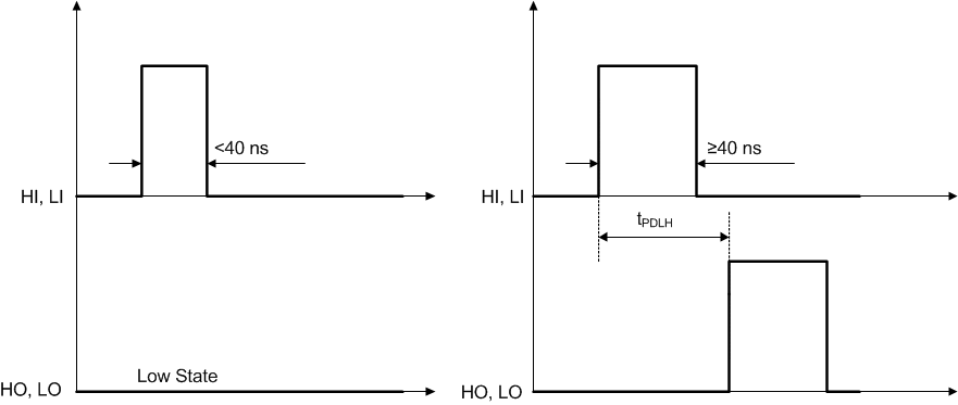
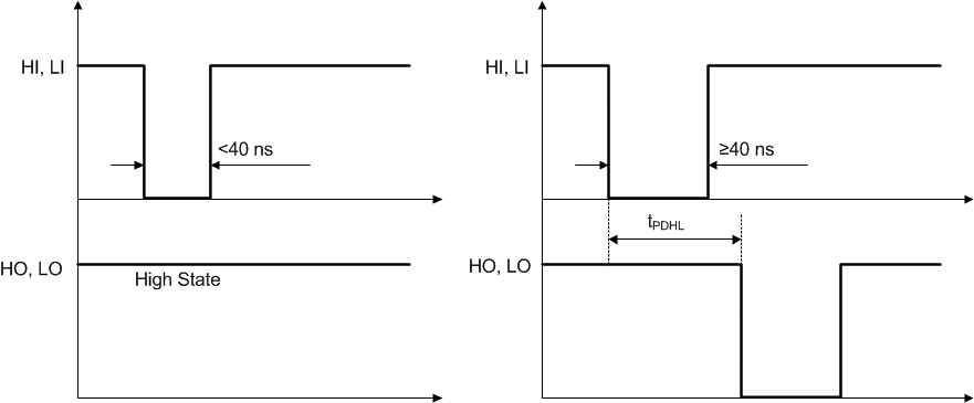
The UCC27710 device has a minimum turn-on, turn-off pulse transfer function to the output pin from the input pin. This function ensures UCC27710 is in the correct state when the input signal is very narrow. The function is summarized in Figure 36 and Figure 37. The tON which is 40 ns typical is shown in Figure 36 and tOFF which is 40 ns typical is shown in Figure 37
 Figure 36. Minimum Turn-On Pulse
  Figure 37. Minimum Turn-Off Pulse