SLUSCE9B June 2017 – March 2020 UCC27712
PRODUCTION DATA.
- 1 Features
- 2 Applications
- 3 Description
- 4 Revision History
- 5 Pin Configuration and Functions
- 6 Specifications
- 7 Detailed Description
-
8 Application and Implementation
- 8.1 Application Information
- 8.2
Typical Application
- 8.2.1 Design Requirements
- 8.2.2
Detailed Design Procedure
- 8.2.2.1 Selecting HI and LI Low Pass Filter Components (RHI, RLI, CHI, CLI)
- 8.2.2.2 Selecting Bootstrap Capacitor (CBOOT)
- 8.2.2.3 Selecting VDD Bypass/Holdup Capacitor (CVDD) and Rbias
- 8.2.2.4 Selecting Bootstrap Resistor (RBOOT)
- 8.2.2.5 Selecting Gate Resistor RON/ROFF
- 8.2.2.6 Selecting Bootstrap Diode
- 8.2.2.7 Estimate the UCC27712 Power Losses (PUCC27712)
- 8.2.2.8 Estimating Junction Temperature
- 8.2.2.9 Operation With IGBT's
- 8.2.3 Application Curves
- 9 Power Supply Recommendations
- 10Layout
- 11Device and Documentation Support
- 12Mechanical, Packaging, and Orderable Information
Package Options
Mechanical Data (Package|Pins)
- D|8
Thermal pad, mechanical data (Package|Pins)
Orderable Information
7.3.3 Input Stage
The input pins of UCC27712 are based on a TTL and CMOS compatible input-threshold logic that is independent of the VDD supply voltage. With typical high threshold (VINH) of 2.0 V and typical low threshold (VINL) of 1.2 V, along with very little temperature variation as summarized in Figure 16 and Figure 17, the input pins are conveniently driven with logic level PWM control signals derived from 3.3-V and 5-V digital power-controller devices. Wider hysteresis (typically 0.8 V) offers enhanced noise immunity compared to traditional TTL logic implementations, where the hysteresis is typically less than 0.5 V. UCC27712 also features tight control of the input pin threshold voltage levels which eases system design considerations and ensures stable operation across temperature.
The UCC27712 includes an important feature: wherein, whenever any of the input pins is in a floating condition, the output of the respective channel is held in the low state. This is achieved using COM pull-down resistors on all the input pins (HI, LI).
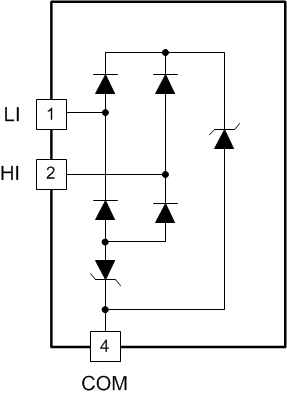
The UCC27712 input pins are capable of sustaining voltages higher than the bias voltage applied on the VDD pin of the device, as long as the absolute magnitude is less than the recommended operating condition's maximum ratings. This features offers the convenience of driving the PWM controller at a higher VDD bias voltage than the UCC27712 helping to reduce gate charge related switching losses. This capability is envisaged in UCC27712 by way of two ESD diodes tied back-to-front as shown in Figure 31.
Additionally, the input pins are also capable of sustaining negative voltages below COM, as long as the magnitude of the negative voltage is less than the recommended operating condition minimum ratings. A similar diode arrangement exists between the input pins and COM as illustrated in Figure 31.
The input stage of each driver must be driven by a signal with a short rise or fall time. This condition is satisfied in typical power supply applications, when the input signals are provided by a PWM controller or logic gates with fast transition times. With a slow changing input voltage, the output of driver may switch repeatedly at a high frequency. While the wide hysteresis offered in UCC27712 definitely alleviates this concern over most other TTL input threshold devices, extra care is necessary in these implementations. If limiting the rise or fall times to the power device is the primary goal, then an external resistance is highly recommended between the output of the driver and the power device. This external resistor has the additional benefit of reducing part of the gate-charge related power dissipation in the gate-driver device package and transferring it into the external resistor itself. If an RC filter is to be added on the input pins for reducing the impact of system noise and ground bounce, the time constant of the RC filter is recommended to be 20 ns or less, for example, 50 Ω with 220 pF is an acceptable choice.
 Figure 31. Diode Structure of Input Stage