SLUSCE9B June 2017 – March 2020 UCC27712
PRODUCTION DATA.
- 1 Features
- 2 Applications
- 3 Description
- 4 Revision History
- 5 Pin Configuration and Functions
- 6 Specifications
- 7 Detailed Description
-
8 Application and Implementation
- 8.1 Application Information
- 8.2
Typical Application
- 8.2.1 Design Requirements
- 8.2.2
Detailed Design Procedure
- 8.2.2.1 Selecting HI and LI Low Pass Filter Components (RHI, RLI, CHI, CLI)
- 8.2.2.2 Selecting Bootstrap Capacitor (CBOOT)
- 8.2.2.3 Selecting VDD Bypass/Holdup Capacitor (CVDD) and Rbias
- 8.2.2.4 Selecting Bootstrap Resistor (RBOOT)
- 8.2.2.5 Selecting Gate Resistor RON/ROFF
- 8.2.2.6 Selecting Bootstrap Diode
- 8.2.2.7 Estimate the UCC27712 Power Losses (PUCC27712)
- 8.2.2.8 Estimating Junction Temperature
- 8.2.2.9 Operation With IGBT's
- 8.2.3 Application Curves
- 9 Power Supply Recommendations
- 10Layout
- 11Device and Documentation Support
- 12Mechanical, Packaging, and Orderable Information
Package Options
Mechanical Data (Package|Pins)
- D|8
Thermal pad, mechanical data (Package|Pins)
Orderable Information
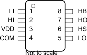
5 Pin Configuration and Functions
D Package
8-Pin SOIC
Top View

Pin Functions
| PIN | I/O | DESCRIPTION | ||
|---|---|---|---|---|
| NAME | NO. | |||
| COM | 4 | – | Ground | |
| HB | 8 | I | High-side floating supply. Bypass this pin to HS with a suitable capacitor to sustain boot-strap circuit operation, typically 10 times bigger than the MOSFETs/IGBTs gate capacitance. | |
| HI | 2 | I | Logic input for high-side driver. If HI is unbiased or floating, HO is held low | |
| HO | 7 | O | High-side driver output. | |
| HS | 6 | – | Return for high-side floating supply. | |
| LI | 1 | I | Logic input for low-side driver. If LI is unbiased or floating, LO is held low | |
| LO | 5 | O | Low-side driver output. | |
| VDD | 3 | I | Bias supply input. Power supply for the input logic side of the device and also low-side driver output. Bypass this pin to COM with a 0.1-µF or larger value ceramic capacitor. | |