SLUS161G April 1999 – April 2025 UCC2813-0 , UCC2813-1 , UCC2813-2 , UCC2813-3 , UCC2813-4 , UCC2813-5 , UCC3813-0 , UCC3813-1 , UCC3813-2 , UCC3813-3 , UCC3813-4 , UCC3813-5
PRODUCTION DATA
- 1
- 1 Features
- 2 Applications
- 3 Description
- 4 Device Comparison Table
- 5 Pin Configuration and Functions
- 6 Specifications
-
7 Detailed Description
- 7.1 Overview
- 7.2 Functional Block Diagram
- 7.3
Feature Description
- 7.3.1 Detailed Pin Descriptions
- 7.3.2 Undervoltage Lockout (UVLO)
- 7.3.3 Self-Biasing, Active Low Output
- 7.3.4 Reference Voltage
- 7.3.5 Oscillator
- 7.3.6 Synchronization
- 7.3.7 PWM Generator
- 7.3.8 Minimum Off-Time Adjustment (Dead-Time Control)
- 7.3.9 Leading Edge Blanking
- 7.3.10 Minimum Pulse Width
- 7.3.11 Current Limiting
- 7.3.12 Overcurrent Protection and Full-Cycle Restart
- 7.3.13 Soft Start
- 7.3.14 Slope Compensation
- 7.4 Device Functional Modes
-
8 Application and Implementation
- 8.1 Application Information
- 8.2
Typical Application
- 8.2.1 Design Requirements
- 8.2.2
Detailed Design Procedure
- 8.2.2.1 Bulk Capacitor Calculation
- 8.2.2.2 Transformer Design
- 8.2.2.3 MOSFET and Output Diode Selection
- 8.2.2.4 Output Capacitor Calculation
- 8.2.2.5 Current Sensing Network
- 8.2.2.6 Gate Drive Resistor
- 8.2.2.7 REF Bypass Capacitor
- 8.2.2.8 RT and CT
- 8.2.2.9 Start-Up Circuit
- 8.2.2.10 Voltage Feedback Compensation Procedure
- 8.2.3 Application Curves
- 8.3 Power Supply Recommendations
- 8.4 Layout
- 9 Device and Documentation Support
- 10Revision History
- 11Mechanical, Packaging, and Orderable Information
Package Options
Refer to the PDF data sheet for device specific package drawings
Mechanical Data (Package|Pins)
- D|8
- PW|8
Thermal pad, mechanical data (Package|Pins)
Orderable Information
8.2.2.10.2 Compensating the Loop
For good transient response, the bandwidth of the finalized design must be as wide as possible. The bandwidth of a CCM flyback (fBW) is limited to ¼ of the RHP-zero frequency, or approximately 1.9 kHz using Equation 33.

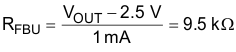
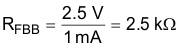
The gain of the open-loop power stage at fBW is equal to –22.4 dB and the phase at fBW is equal to –87°. First step is to choose the output voltage-sensing resistor values. The output sensing resistors are selected based on the allowed power consumption and in this case, 1 mA of sensing current is assumed.
The TL431 is used as the feedback amplifier. Given its 2.5-V reference voltage, the voltage-sensing dividers RFBU and RFBB can be selected with Equation 34 and Equation 35.
Next step is to put the compensator zero fCZ at 190 Hz, which is 1/10 of the target crossover frequency. Choose CZ as a fixed value of 10 nF and choose the zero resistor value according to Equation 36.

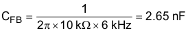
Next, place a pole at the lower of RHP-zero or the ESR-zero frequencies. Based previous analysis, the RHP zero is at 7.65 kHz and the ESR zero is at 6 kHz, so the pole of the compensation loop should be put at 6 kHz. This pole can be added through the primary side error amplifier. RFB and CFB provide the necessary pole. Choosing RFB as 10 kΩ, CFB is calculated by Equation 37.
Based on the compensation loop structure, the entire compensation loop transfer function is written as Equation 38.

where
- CTR is the current transfer ratio of the opto-coupler. Choose 1 as the nominal value for CTR.
- REG is the opto-emitter pulldown resistor and 1 kΩ is chosen as a default value
The only remaining unknown value required in this equation is RLED. The entire loop gain must be equal to 1 at the crossover frequency. RLED is calculated accordingly as 1.62 kΩ.
The final closed-loop Bode plots are shown in Figure 8-4 and Figure 8-5. The converter achieves approximately 2-kHz crossover frequency and approximately 70° of phase margin.
TI recommends checking the loop stability across all the corner cases, including component tolerances, to ensure system stability.
 Figure 8-4 Converter Closed-Loop Bode Plot: Gain
 Figure 8-5 Converter Closed-Loop Bode Plot: Phase