SLUSC61A January 2015 – December 2020 UCC28700-Q1
PRODUCTION DATA
- 1 Features
- 2 Applications
- 3 Description
- 4 Revision History
- 5 Pin Configuration and Functions
- 6 Specifications
- 7 Detailed Description
-
8 Applications and Implementation
- 8.1 Application Information
- 8.2
Typical Application
- 8.2.1 Design Requirements
- 8.2.2
Detailed Design Procedure
- 8.2.2.1 Transformer Parameter Verification
- 8.2.2.2 Output Capacitance
- 8.2.2.3 VDD Capacitance, CDD
- 8.2.2.4 VDD Start-Up Resistance, RSTR
- 8.2.2.5 VS Resistor Divider, Line Compensation, and Cable Compensation
- 8.2.2.6 Input Bulk Capacitance and Minimum Bulk Voltage
- 8.2.2.7 Transformer Turns Ratio, Inductance, Primary-Peak Current
- 8.2.2.8 Standby Power Estimate
- 8.2.3 Application Curves
- 9 Power Supply Recommendations
- 10Layout
-
11Device and Documentation Support
- 11.1
Device Support
- 11.1.1
Device Nomenclature
- 11.1.1.1 Capacitance Terms in Farads
- 11.1.1.2 Duty Cycle Terms
- 11.1.1.3 Frequency Terms in Hertz
- 11.1.1.4 Current Terms in Amperes
- 11.1.1.5 Current and Voltage Scaling Terms
- 11.1.1.6 Transformer Terms
- 11.1.1.7 Power Terms in Watts
- 11.1.1.8 Resistance Terms in Ω
- 11.1.1.9 Timing Terms in Seconds
- 11.1.1.10 Voltage Terms in Volts
- 11.1.1.11 AC Voltage Terms in VRMS
- 11.1.1.12 Efficiency Terms
- 11.1.1
Device Nomenclature
- 11.2 Documentation Support
- 11.3 Trademarks
- 11.1
Device Support
Package Options
Mechanical Data (Package|Pins)
- DBV|6
Thermal pad, mechanical data (Package|Pins)
Orderable Information
3 Description
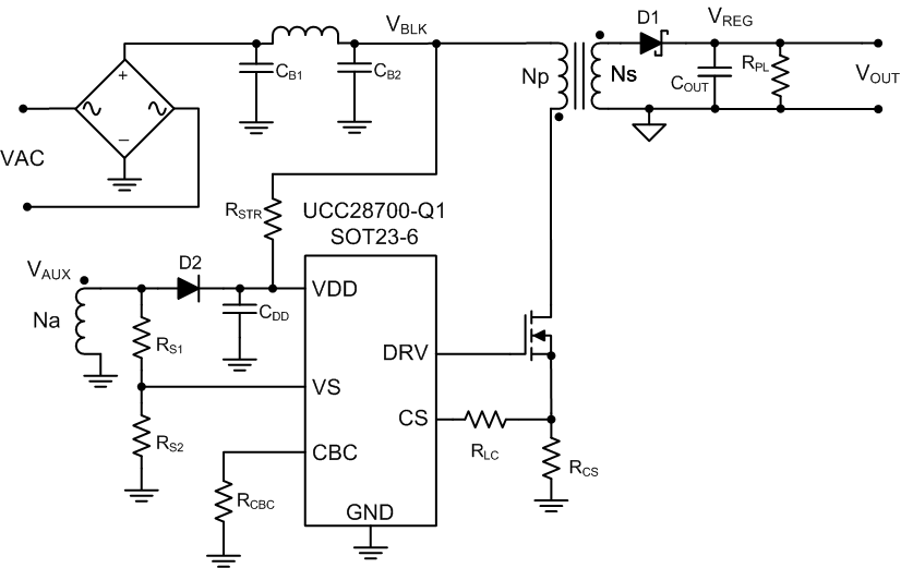
The UCC28700-Q1 of flyback power supply controllers provides Constant-Voltage (CV) and Constant-Current (CC) output regulation without the use of an optical coupler. The devices process information from the primary power switch and an auxiliary flyback winding for precise control of output voltage and current. Low start-up current, dynamically controlled operating states and a tailored modulation profile support very low standby power without sacrificing start-up time or output transient response.
Control algorithms in the UCC28700-Q1 allows operating efficiencies to meet or exceed applicable standards. The output drive interfaces to a MOSFET power switch. Discontinuous Conduction Mode (DCM) with valley switching reduces switching losses. Modulation of switching frequency and primary current peak amplitude (FM and AM) keeps the conversion efficiency high across the entire load and line ranges.
The controllers have a maximum switching frequency of 130 kHz and always maintain control of the peak-primary current in the transformer. Protection features help keep primary and secondary component stresses in check. The UCC28700-Q1 allows the level of cable compensation to be programmed.
| PART NUMBER | PACKAGE | BODY SIZE (NOM) |
|---|---|---|
| UCC28700-Q1 | SOT-23 (6) | 2.90 mm × 1.60 mm |
 Typical Application
Schematic