SLUS829G August   2008  – February 2020 UCC2897A

PRODUCTION DATA.  

  1. Features
  2. Applications
  3. Description
    1.     Device Images
      1.      Typical Application Diagram
  4. Revision History
  5. Device Options
  6. Pin Configuration and Functions
    1.     Pin Functions
  7. Specifications
    1. 7.1 Absolute Maximum Ratings
    2. 7.2 ESD Ratings
    3. 7.3 Recommended Operating Conditions
    4. 7.4 Thermal Information
    5. 7.5 Electrical Characteristics
    6. 7.6 Timing Requirements
    7. 7.7 Typical Characteristics
  8. Detailed Description
    1. 8.1 Overview
    2. 8.2 Functional Block Diagram
    3. 8.3 Feature Description
      1. 8.3.1 Detailed Pin Descriptions
        1. 8.3.1.1  RDEL
        2. 8.3.1.2  RON
        3. 8.3.1.3  ROFF
        4. 8.3.1.4  VREF
        5. 8.3.1.5  SYNC
        6. 8.3.1.6  GND
        7. 8.3.1.7  CS
        8. 8.3.1.8  RSLOPE
        9. 8.3.1.9  FB
        10. 8.3.1.10 SS/SD
        11. 8.3.1.11 PGND
        12. 8.3.1.12 AUX
        13. 8.3.1.13 OUT
        14. 8.3.1.14 VDD
        15. 8.3.1.15 LINEUV
        16. 8.3.1.16 VIN
        17. 8.3.1.17 LINEOV
      2. 8.3.2 JFET Control and UVLO
      3. 8.3.3 Line Undervoltage Protection
      4. 8.3.4 Line Overvoltage Protection
      5. 8.3.5 Pulse Skipping
      6. 8.3.6 Synchronization
      7. 8.3.7 Gate Drive Connection
      8. 8.3.8 Bootstrap Biasing
    4. 8.4 Device Functional Modes
  9. Application and Implementation
    1. 9.1 Application Information
    2. 9.2 Typical Application
      1. 9.2.1 Design Requirements
      2. 9.2.2 Detailed Design Procedure
        1. 9.2.2.1 Oscillator
        2. 9.2.2.2 Soft Start
        3. 9.2.2.3 VDD Bypass Requirements
        4. 9.2.2.4 Delay Programming
        5. 9.2.2.5 Input Voltage Monitoring
        6. 9.2.2.6 Current Sense and Slope Compensation
      3. 9.2.3 Application Curves
  10. 10Power Supply Recommendations
  11. 11Layout
    1. 11.1 Layout Guidelines
    2. 11.2 Layout Example
  12. 12Device and Documentation Support
    1. 12.1 Documentation Support
      1. 12.1.1 Related Documentation
    2. 12.2 Receiving Notification of Documentation Updates
    3. 12.3 Community Resources
    4. 12.4 Trademarks
    5. 12.5 Electrostatic Discharge Caution
    6. 12.6 Glossary
  13. 13Mechanical, Packaging, and Orderable Information

Package Options

Mechanical Data (Package|Pins)
Thermal pad, mechanical data (Package|Pins)
Orderable Information

Device Functional Modes

The UCC2897A uses a high voltage JFET to provide the start-up current for the controller until a bootstrap-type rail becomes available on VDD pin. The JFET will be turned off after the VDD pin voltage exceeds the UVLO threshold. Then the device enters normal operation mode. If the line voltage is abnormal, the device enters line under voltage or line over voltage mode. During light load or load transient, the device may enter pulse skipping mode if the feedback voltage FB is less than a certain threshold. Figure 27 shows the mode transition diagram.
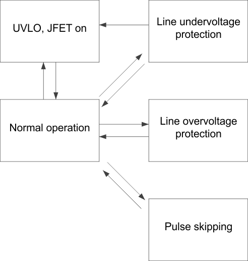
UCC2897A Modetransitiondiagram.gifFigure 27. Mode Transition Diagram