SLLSER8J June 2017 – August 2024 UCC5310 , UCC5320 , UCC5350 , UCC5390
PRODUCTION DATA
- 1
- 1 Features
- 2 Applications
- 3 Description
- 4 Device Comparison Table
- 5 Pin Configuration and Function
-
6 Specifications
- 6.1 Absolute Maximum Ratings
- 6.2 ESD Ratings
- 6.3 Recommended Operating Conditions
- 6.4 Thermal Information
- 6.5 Power Ratings
- 6.6 Insulation Specifications for D Package
- 6.7 Insulation Specifications for DWV Package
- 6.8 Safety-Related Certifications For D Package
- 6.9 Safety-Related Certifications For DWV Package
- 6.10 Safety Limiting Values
- 6.11 Electrical Characteristics
- 6.12 Switching Characteristics
- 6.13 Insulation Characteristics Curves
- 6.14 Typical Characteristics
- 7 Parameter Measurement Information
- 8 Detailed Description
- 9 Application and Implementation
- 10Power Supply Recommendations
- 11Layout
- 12Device and Documentation Support
- 13Revision History
- 14Mechanical, Packaging, and Orderable Information
Package Options
Refer to the PDF data sheet for device specific package drawings
Mechanical Data (Package|Pins)
- D|8
- DWV|8
Thermal pad, mechanical data (Package|Pins)
Orderable Information
9.2.2.2 Gate-Driver Output Resistor
The external gate-driver resistors, RG(ON) and RG(OFF) are used to:
- Limit ringing caused by parasitic inductances and capacitances
- Limit ringing caused by high voltage or high current switching dv/dt, di/dt, and body-diode reverse recovery
- Fine-tune gate drive strength, specifically peak sink and source current to optimize the switching loss
- Reduce electromagnetic interference (EMI)
The output stage has a pull-up structure consisting of a P-channel MOSFET and an N-channel MOSFET in parallel. The combined peak source current is 4.3 A for the UCC5320 family and 17 A for the UCC5390 family and 17 A for the UCC5390 family. Use Equation 1 to estimate the peak source current using the UCC5320S as an example.
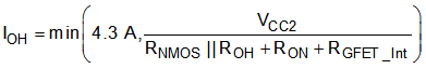
where
- RON is the external turn-on resistance.
- RGFET_Int is the power transistor internal gate resistance, found in the power transistor data sheet. We will assume 0Ω for our example.
- IOH is the peak source current which is the minimum value between 4.3 A, the gate-driver peak source current, and the calculated value based on the gate-drive loop resistance.
In this example, the peak source current is approximately 1.8 A as calculated in Equation 2.

Similarly, use Equation 3 to calculate the peak sink current.

where
- ROFF is the external turn-off resistance.
- IOL is the peak sink current which is the minimum value between 4.4 A, the gate-driver peak sink current, and the calculated value based on the gate-drive loop resistance.
In this example, the peak sink current is the minimum value between Equation 4 and 4.4 A.

The estimated peak current is also influenced by PCB layout and load capacitance. Parasitic inductance in the gate-driver loop can slow down the peak gate-drive current and introduce overshoot and undershoot. Therefore, TI strongly recommends that the gate-driver loop should be minimized. Conversely, the peak source and sink current is dominated by loop parasitics when the load capacitance (CISS) of the power transistor is very small (typically less than 1 nF) because the rising and falling time is too small and close to the parasitic ringing period.