SLUSC66E March   2015  – February 2017 UCD3138A

PRODUCTION DATA.  

  1. Device Overview
    1. 1.1 Features
    2. 1.2 Applications
    3. 1.3 Description
    4. 1.4 Functional Block Diagram
  2. Device Comparison
    1. 2.1 Product Selection Matrix
  3. Pin Configuration and Functions
    1. 3.1 UCD3138A RGC Package
    2. 3.2 UCD3138A RMH Package
    3. 3.3 UCD3138A RJA Package
  4. Specifications
    1. 4.1 Absolute Maximum Ratings
    2. 4.2 ESD Ratings
    3. 4.3 Recommended Operating Conditions
    4. 4.4 Thermal Information
    5. 4.5 Electrical Characteristics
    6. 4.6 PMBus/SMBus/I2C Timing
    7. 4.7 Peripherals
      1. 4.7.1 Digital Power Peripherals (DPPs)
        1. 4.7.1.1 Front End
        2. 4.7.1.2 DPWM Module
        3. 4.7.1.3 DPWM Events
        4. 4.7.1.4 High Resolution DPWM
        5. 4.7.1.5 Oversampling
        6. 4.7.1.6 DPWM Interrupt Generation
        7. 4.7.1.7 DPWM Interrupt Scaling/Range
        8. 4.7.1.8 DPWM Synchronization
        9. 4.7.1.9 Synchronous Rectifier Dead-Time Optimization Peripheral
    8. 4.8 Typical Temperature Characteristics
  5. Parametric Measurements Information
    1. 5.1 Power-On Reset (POR) and Brown-Out Reset (BOR)
  6. Detailed Description
    1. 6.1 Overview
    2. 6.2 ARM Processor
    3. 6.3 Memory
      1. 6.3.1 CPU Memory Map and interruptions
      2. 6.3.2 Boot ROM
      3. 6.3.3 Customer Boot Program
      4. 6.3.4 Flash Management
    4. 6.4 System Module
      1. 6.4.1 Address Decoder (DEC)
      2. 6.4.2 Memory Management Controller (MMC)
      3. 6.4.3 System Management (SYS)
      4. 6.4.4 Central Interrupt Module (CIM)
    5. 6.5 Feature Description
      1. 6.5.1  Sync FET Ramp and IDE Calculation
      2. 6.5.2  Automatic Mode Switching
        1. 6.5.2.1 Phase Shifted Full Bridge Example
        2. 6.5.2.2 LLC Example
        3. 6.5.2.3 Mechanism for Automatic Mode Switching
      3. 6.5.3  DPWMC, Edge Generation, IntraMux
      4. 6.5.4  Filter
        1. 6.5.4.1 Loop Multiplexer
        2. 6.5.4.2 Fault Multiplexer
      5. 6.5.5  Communication Ports
        1. 6.5.5.1 SCI (UART) Serial Communication Interface
        2. 6.5.5.2 PMBus Interfacte
        3. 6.5.5.3 General Purpose ADC12
        4. 6.5.5.4 Timers
          1. 6.5.5.4.1 24-bit PWM Timer
          2. 6.5.5.4.2 16-Bit PWM Timers
          3. 6.5.5.4.3 Watchdog Timer
      6. 6.5.6  Miscellaneous Analog
      7. 6.5.7  Package ID Information
      8. 6.5.8  Brownout
      9. 6.5.9  Global I/O
      10. 6.5.10 Temperature Sensor Control
      11. 6.5.11 I/O Mux Control
      12. 6.5.12 Current Sharing Control
      13. 6.5.13 Temperature Reference
  7. Device Functional Modes
    1. 7.1 Normal Mode
    2. 7.2 DPWM Multiple Output Mode
    3. 7.3 DPWM Resonant Mode
    4. 7.4 Triangular Mode
    5. 7.5 Leading Edge Mode
  8. Application and Implementation
    1. 8.1 Application Information
    2. 8.2 Typical Application
      1. 8.2.1 Design Requirements
      2. 8.2.2 Detailed Design Procedure
        1. 8.2.2.1 PCMC (Peak Current Mode Control) PSFB (Phase-Shifted Full Bridge) Hardware Configuration Overview
        2. 8.2.2.2 DPWM Initialization for PSFB
      3. 8.2.3 Fixed Signals to Bridge
      4. 8.2.4 Dynamic Signals to Bridge
      5. 8.2.5 System Initialization for PCM
        1. 8.2.5.1 Use of Front Ends and Filters in PSFB
        2. 8.2.5.2 Peak Current Detection
        3. 8.2.5.3 Peak Current Mode (PCM)
      6. 8.2.6 Application Curves
  9. Power Supply Recommendations
    1. 9.1 Power Supply Decoupling and Bulk Capacitors
  10. 10Layout
    1. 10.1 Layout Guidelines
    2. 10.2 Layout Example
  11. 11Device and Documentation Support
    1. 11.1 Device Support
      1. 11.1.1 Development Support
        1. 11.1.1.1 Tools and Documentation
    2. 11.2 Documentation Support
      1. 11.2.1 References
    3. 11.3 Receiving Notification of Documentation Updates
    4. 11.4 Community Resources
    5. 11.5 Trademarks
    6. 11.6 Electrostatic Discharge Caution
    7. 11.7 Glossary
  12. 12Mechanical Packaging and Orderable Information
    1. 12.1 Packaging Information

Package Options

Mechanical Data (Package|Pins)
Thermal pad, mechanical data (Package|Pins)
Orderable Information

Layout

Layout Guidelines

  • Single ground is recommended: SGND. A multilayer such as 4 layers board is recommended so that one solid SGND is dedicated for return current path, referred to the layout example.
  • Apply multiple different capacitors for different frequency range on decoupling circuits. Each capacitor has different ESL, Capacitance and ESR, and they have different frequency response.
  • Avoid long traces close to radiation components, and place them into an internal layer, and it is preferred to have grounding shield, and in the end, add a termination circuit;
  • Analog circuit such as ADC sensing lines needs a return current path into the analog circuitry; digital circuit such as GPIO, PMBus and PWM has a return current path into the digital circuitry; although with a single plane, still try to avoid to mix analog current and digital current.
  • Don’t use a ferrite bead or larger than 3-Ω resistor to connect between V33A and V33D.
  • Both 3.3VD and 3.3VA should have local 4.7-µF decoupling capacitors close to the device power pins, add visas to connect decoupling caps directly to SGND.
  • Avoid negative current/negative voltage on all pins, so Schottky diodes may need to clamp the voltage; avoid the voltage spike on all pins more than 3.8 V or less than –0.3 V, add Schottky diodes on the pins which could have voltage spikes during surge test; be aware that a Schottky has relatively higher leakage current, which can affect the voltage sensing at high temperature.
  • If V33 slew rate is less than 2.5 V/ms the RESET pin should have a 2.21-kΩ resistor between the reset pin and V33D and a 2.2-µF capacitor from RESET to ground. For more details please refer to the UCD3138 Family - Practical Design Guideline This capacitor must be located close to the device RESET pin.
  • 2.2 µF between V33D and BP18 can be removed due to internal enhancement design.
  • Configure unused GPIO pins to be inputs or connect them to the ground (DGND or SGND). For detailed practical design guideline refer to UCD3138 Family - Practical Design Guideline
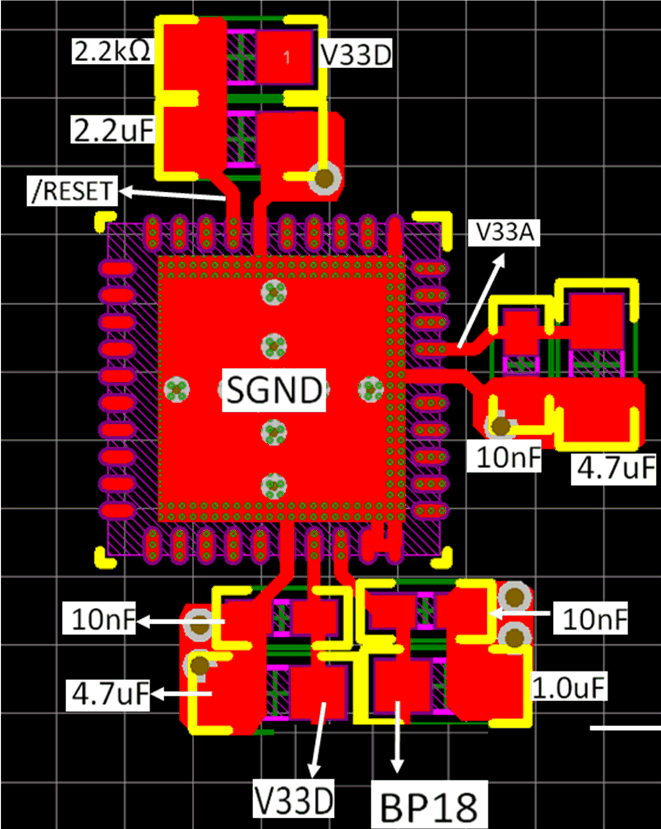
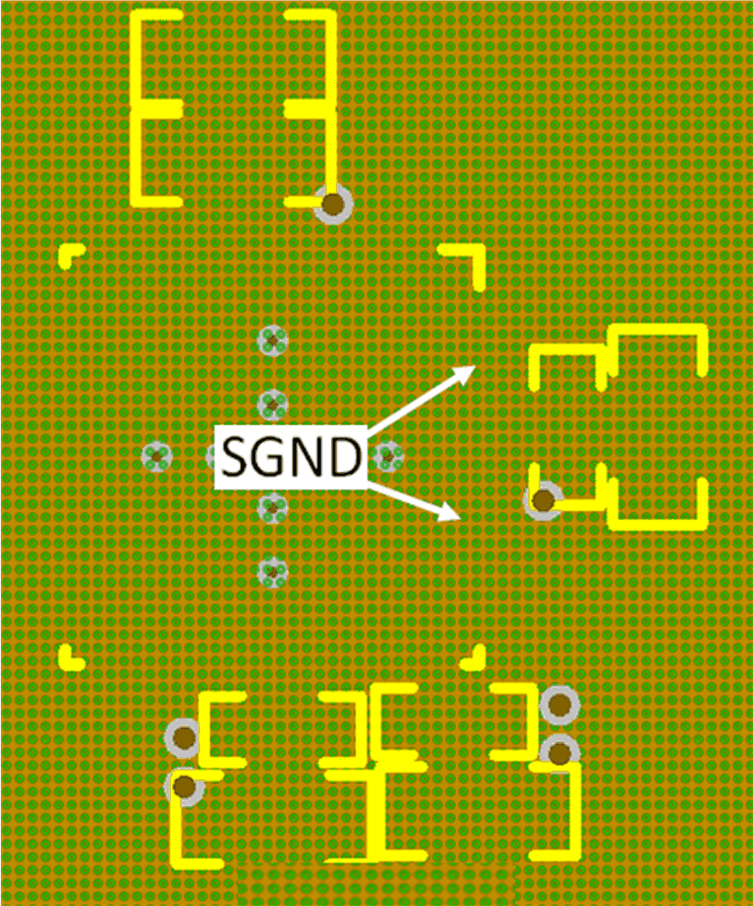
Layout Example

UCD3138A de2_lusc66.gif Figure 10-1 UCD3138A Layout Example
UCD3138A de3_lusc66.gif Figure 10-2 UCD3138A Layout Example, Internal Plane