SLUSC66E March 2015 – February 2017 UCD3138A
PRODUCTION DATA.
- 1 Device Overview
- 2 Device Comparison
- 3 Pin Configuration and Functions
- 4 Specifications
- 5 Parametric Measurements Information
-
6 Detailed Description
- 6.1 Overview
- 6.2 ARM Processor
- 6.3 Memory
- 6.4 System Module
- 6.5
Feature Description
- 6.5.1 Sync FET Ramp and IDE Calculation
- 6.5.2 Automatic Mode Switching
- 6.5.3 DPWMC, Edge Generation, IntraMux
- 6.5.4 Filter
- 6.5.5 Communication Ports
- 6.5.6 Miscellaneous Analog
- 6.5.7 Package ID Information
- 6.5.8 Brownout
- 6.5.9 Global I/O
- 6.5.10 Temperature Sensor Control
- 6.5.11 I/O Mux Control
- 6.5.12 Current Sharing Control
- 6.5.13 Temperature Reference
- 7 Device Functional Modes
- 8 Application and Implementation
- 9 Power Supply Recommendations
- 10Layout
- 11Device and Documentation Support
- 12Mechanical Packaging and Orderable Information
Package Options
Mechanical Data (Package|Pins)
Thermal pad, mechanical data (Package|Pins)
Orderable Information
7 Device Functional Modes
The DPWM is a complex logic system which is highly configurable to support several different power supply topologies. This section discusses waveforms, timing, and register settings, rather than ON-logic design.
The DPWM functions using a period counter, which increments from 0 to PRD, then resets and begins to increment again.
The DPWM logic causes transitions in many digital signals when the period counter reaches the target value for that signal.
7.1 Normal Mode
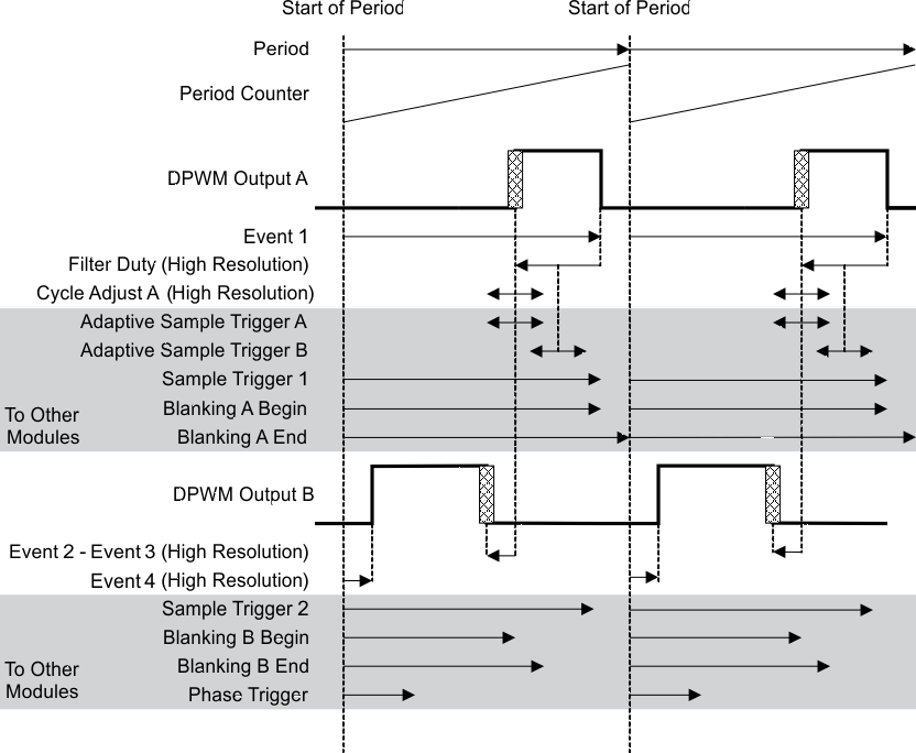
In Normal mode, the Filter output determines the pulse width on DPWM A. DPWM B fits into the rest of the switching period, with a dead time separating it from the DPWM A on-time. It is useful for buck topologies. The drawing of the Normal Mode waveforms is shown in Figure 7-17.
Cycle adjust A can be used to adjust pulse widths on individual phases of a multi-phase system. This can be used for functions like current balancing. The Adaptive Sample Triggers can be used to sample in the middle of the on-time (for an average output), or at the end of the on-time (to minimize phase delay) The Adaptive Sample Register provides an offset from the center of the on-time. This can compensate for external delays, such as MOSFET and gate driver turn on times.
Blanking A-Begin and Blanking A-End can be used to blank out noise from the MOSFET turn on at the beginning of the period (DPWMA rising edge). Blanking B could be used at the turn off time of DPWMB. The other edges are dynamic, so blanking is more difficult.
Cycle Adjust B has no effect in Normal Mode.
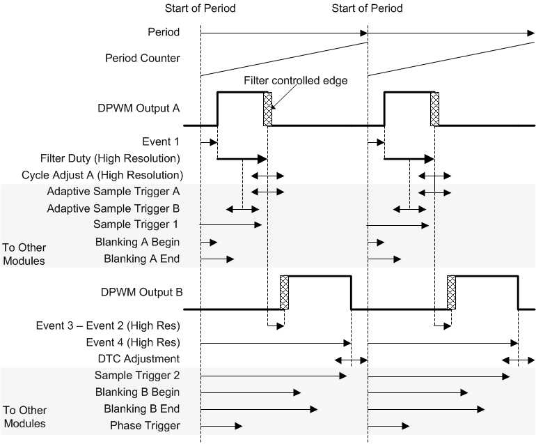
- DPWM A Rising Edge = Event 1
- DPWM A Falling Edge = Event 1 + Filter Duty + Cycle Adjust A
- Adaptive Sample Trigger A = Event 1 + Filter Duty + Adaptive Sample Register or
- Adaptive Sample Trigger B = Event 1 + Filter Duty/2 + Adaptive Sample Register
- DPWM B Rising Edge = Event 1 + Filter Duty + Cycle Adjust A + (Event 3 – Event 2)
- DPWM B Falling Edge = Event 4 + DTC Adjustment
- Phase Trigger = Phase Trigger Register value or Filter Duty
Events always set by their registers, regardless of mode:
- Sample Trigger 1, Sample Trigger 2, Blanking A Begin, Blanking A End, Blanking B
- Begin, Blanking B End
7.2 DPWM Multiple Output Mode
The device uses multi-mode functionality in systems where each phase has only one driver signal. It enables each DPWM peripheral to drive two phases with the same pulse width, but with a time offset between the phases, and with different cycle adjusts for each phase.
The diagram for Multi-Mode is shown in Figure 7-18.
Event 2 and Event 4 are not relevant in Multi mode.
DPWMB can cross over the period boundary safely, and still have the proper pulse width, so full 100% pulse width operation is possible. DPWMA cannot cross over the period boundary.
Since the rising edge on DPWM B is also fixed, Blanking B-Begin and Blanking B-End can be used for blanking this rising edge.
Cycle Adjust B is usable on DPWM B.
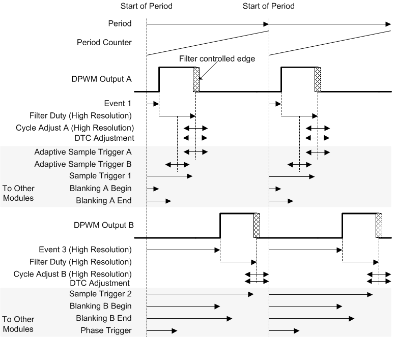
- DPWM A Rising Edge = Event 1
- DPWM A Falling Edge = Event 1 + Filter Duty + Cycle Adjust A + DTC Adjustment
- Adaptive Sample Trigger A = Event 1 + Filter Duty + Adaptive Sample Register or
- Adaptive Sample Trigger B = Event 1 + Filter Duty/2 + Adaptive Sample Register
- DPWM B Rising Edge = Event 3
- DPWM B Falling Edge = Event 3 + Filter Duty + Cycle Adjust B + DTC Adjustment
- Phase Trigger = Phase Trigger Register value or Filter Duty
Events always set by their registers, regardless of mode:
- Sample Trigger 1, Sample Trigger 2, Blanking A Begin, Blanking A End, Blanking B
- Begin, Blanking B End
7.3 DPWM Resonant Mode
This mode provides a symmetrical waveform where DPWMA and DPWMB have the same pulse width. As the switching frequency changes, the dead times between the pulses remain the same.
The equations for this mode are designed for a smooth transition from PWM mode to resonant mode, as described in Section 6.5.2.2. The diagram of this mode is shown in Figure 7-19.
The filter has two outputs, filter duty and filter period. In this case, the Filter is configured so that the filter period is twice the filter duty. So when there were no dead times, each DPWM pin in ON for half of the period. For dead-time handling, the device substracts the average of the two dead times from the filter duty for both DPWM pins. Therefore, both pins have the same ON-time, and the dead times are fixed regardless of the period. The only edge which is fixed relative to the start of the period is the rising edge of DPWM A. This is the only edge for which the blanking signals can be used easily.
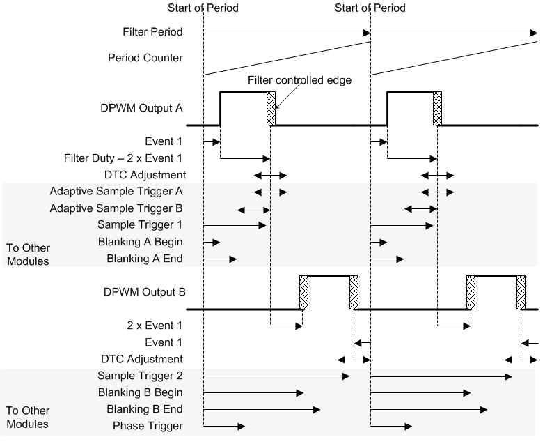
- DPWM A Rising Edge = Event 1
- DPWM A Falling Edge = Filter Duty – Event 1
- Adaptive Sample Trigger A = Event 1 + Filter Duty + Adaptive Sample Register or
- Adaptive Sample Trigger B = Event 1 + Filter Duty/2 + Adaptive Sample Register
- DPWM B Rising Edge = Filter Duty + Event 1
- DPWM B Falling Edge = Filter Period – Event 1
- Phase Trigger = Phase Trigger Register value or Filter Duty
Events always set by their registers, regardless of mode:
- Sample Trigger 1, Sample Trigger 2, Blanking A Begin, Blanking A End, Blanking B
- Begin, Blanking B End
7.4 Triangular Mode
Triangular mode provides a stable phase shift in interleaved PFC and similar topologies. In this case, the PWM pulse is centered in the middle of the period, rather than starting at one end or the other. In Triangular Mode, only DPWM-B is available. The diagram for Triangular Mode is shown in Figure 7-20.
All edges are dynamic in triangular mode, so fixed blanking is not that useful. The adaptive sample trigger is not needed. It is very easy to put a fixed sample trigger exactly in the center of the FET on-time, because the center of the on-time does not move in this mode.
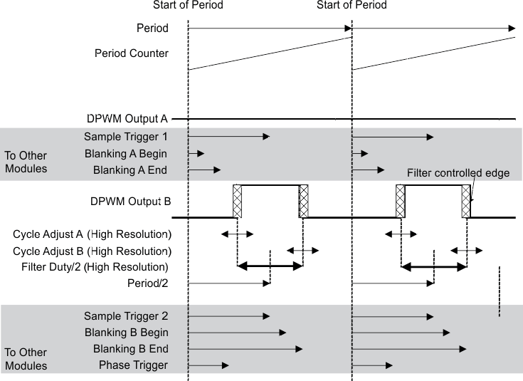
- DPWM A Rising Edge = None
- DPWM A Falling Edge = None
- Adaptive Sample Trigger = None
- DPWM B Rising Edge = Period / 2 - Filter Duty / 2 + Cycle Adjust A
- DPWM B Falling Edge = Period / 2 + Filter Duty / 2 + Cycle Adjust B
- Phase Trigger = Phase Trigger Register value or Filter Duty
Events always set by their registers, regardless of mode:
- Sample Trigger 1, Sample Trigger 2, Blanking A Begin, Blanking A End, Blanking B
- Begin, Blanking B End
7.5 Leading Edge Mode
Leading edge mode is very similar to Normal mode, reversed in time. The DPWM A falling edge is fixed, and the rising edge moves to the left, or backwards in time, as the filter output increases. The DPWM B falling edge stays ahead of the DPWMA rising edge by a fixed dead time. The diagram of the Leading Edge Mode is shown in Figure 7-21.
As in the Normal mode, the two edges in the middle of the period are dynamic, so the fixed blanking intervals are mainly useful for the edges at the beginning and end of the period.
- DPWM A Rising Edge = Event 1
- DPWM A Falling Edge = = Event 1 - Filter Duty + Cycle Adjust A
- Adaptive Sample Trigger A = Event 1 - Filter Duty + Adaptive Sample Register or
- Adaptive Sample Trigger B = Event 1 - Filter Duty / 2 + Adaptive Sample Register
- DPWM B Rising Edge = Event 4
- DPWM B Falling Edge = Event 1 - Filter Duty + Cycle Adjust A - ( Event 2 – Event 3 )
- Phase Trigger = Phase Trigger Register value or Filter Duty
Events always set by their registers, regardless of mode:
- Sample Trigger 1, Sample Trigger 2, Blanking A Begin, Blanking A End, Blanking B
- Begin, Blanking B End