SLUSC66E March 2015 – February 2017 UCD3138A
PRODUCTION DATA.
- 1 Device Overview
- 2 Device Comparison
- 3 Pin Configuration and Functions
- 4 Specifications
- 5 Parametric Measurements Information
-
6 Detailed Description
- 6.1 Overview
- 6.2 ARM Processor
- 6.3 Memory
- 6.4 System Module
- 6.5
Feature Description
- 6.5.1 Sync FET Ramp and IDE Calculation
- 6.5.2 Automatic Mode Switching
- 6.5.3 DPWMC, Edge Generation, IntraMux
- 6.5.4 Filter
- 6.5.5 Communication Ports
- 6.5.6 Miscellaneous Analog
- 6.5.7 Package ID Information
- 6.5.8 Brownout
- 6.5.9 Global I/O
- 6.5.10 Temperature Sensor Control
- 6.5.11 I/O Mux Control
- 6.5.12 Current Sharing Control
- 6.5.13 Temperature Reference
- 7 Device Functional Modes
- 8 Application and Implementation
- 9 Power Supply Recommendations
- 10Layout
- 11Device and Documentation Support
- 12Mechanical Packaging and Orderable Information
Package Options
Mechanical Data (Package|Pins)
Thermal pad, mechanical data (Package|Pins)
Orderable Information
3 Pin Configuration and Functions
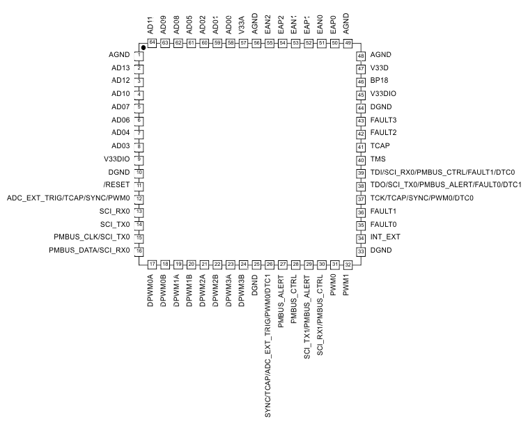
3.1 UCD3138A RGC Package
64 VQFN Package
Top View

UCD3138A RGC Pin Functions
| PIN NO. | NAME | PRIMARY ASSIGNMENT | ALTERNATE ASSIGNMENT | CONFIGURABLE AS A GPIO? |
|||
|---|---|---|---|---|---|---|---|
| NO. 1 | NO. 2 | NO. 3 | NO. 4 | ||||
| 1 | AGND | Analog ground | |||||
| 2 | AD13 | 12-bit ADC, Ch 13, comparator E, I-share | DAC output | ||||
| 3 | AD12 | 12-bit ADC, Ch 12 | |||||
| 4 | AD10 | 12-bit ADC, Ch 10 | |||||
| 5 | AD07 | 12-bit ADC, Ch 7, Connected to comparator F and reference to comparator G | DAC output | ||||
| 6 | AD06 | 12-bit ADC, Ch 6, Connected to comparator F | DAC output | ||||
| 7 | AD04 | 12-bit ADC, Ch 4, Connected to comparator D | DAC output | ||||
| 8 | AD03 | 12-bit ADC, Ch 3, Connected to comparator B and C | |||||
| 9 | V33DIO | Digital I/O 3.3V core supply | |||||
| 10 | DGND | Digital ground | |||||
| 11 | RESET | Device Reset Input, active low | |||||
| 12 | ADC_EXT_TRIG | ADC conversion external trigger input | TCAP | SYNC | PWM0 | Yes | |
| 13 | SCI_RX0 | SCI RX 0 | Yes | ||||
| 14 | SCI_TX0 | SCI TX 0 | Yes | ||||
| 15 | PMBUS_CLK | PMBUS Clock (Open Drain) | SCI TX 0 | Yes | |||
| 16 | PMBUS_DATA | PMBus data (Open Drain) | SCI RX 0 | Yes | |||
| 17 | DPWM0A | DPWM 0A output | Yes | ||||
| 18 | DPWM0B | DPWM 0B output | Yes | ||||
| 19 | DPWM1A | DPWM 1A output | Yes | ||||
| 20 | DPWM1B | DPWM 1B output | Yes | ||||
| 21 | DPWM2A | DPWM 2A output | Yes | ||||
| 22 | DPWM2B | DPWM 2B output | Yes | ||||
| 23 | DPWM3A | DPWM 3A output | Yes | ||||
| 24 | DPWM3B | DPWM 3B output | Yes | ||||
| 25 | DGND | Digital ground | |||||
| 26 | SYNC | DPWM Synchronize pin | TCAP | ADC_EXT_TRIG | PWM0 | DTC1 | Yes |
| 27 | PMBUS_ALERT | PMBus Alert (Open Drain) | Yes | ||||
| 28 | PMBUS_CTRL | PMBus Control (Open Drain) | Yes | ||||
| 29 | SCI_TX1 | SCI TX 1 | PMBUS_ALERT | Yes | |||
| 30 | SCI_RX1 | SCI RX 1 | PMBUS_CTRL | Yes | |||
| 31 | PWM0 | General purpose PWM 0 | Yes | ||||
| 32 | PWM1 | General purpose PWM 1 | Yes | ||||
| 33 | DGND | Digital ground | |||||
| 34 | INT_EXT | External Interrupt | Yes | ||||
| 35 | FAULT0 | External fault input 0 | Yes | ||||
| 36 | FAULT1 | External fault input 1 | Yes | ||||
| 37 | TCK | JTAG TCK | TCAP | SYNC | PWM0 | DTC0 | Yes |
| 38 | TDO | JTAG TDO | SCI_TX0 | PMBUS_ALERT | FAULT0 | DTC1 | Yes |
| 39 | TDI | JTAG TDI | SCI_RX0 | PMBUS_CTRL | FAULT1 | DTC0 | Yes |
| 40 | TMS | JTAG TMS | Yes | ||||
| 41 | TCAP | Timer capture input | Yes | ||||
| 42 | FAULT2 | External fault input 2 | Yes | ||||
| 43 | FAULT3 | External fault input 3 | Yes | ||||
| 44 | DGND | Digital ground | |||||
| 45 | V33DIO | Digital I/O 3.3V core supply | |||||
| 46 | BP18 | 1.8V Bypass | |||||
| 47 | V33D | Digital 3.3V core supply | |||||
| 48 | AGND | Substrate analog ground | |||||
| 49 | AGND | Analog ground | |||||
| 50 | EAP0 | Channel 0, differential analog voltage, positive input | |||||
| 51 | EAN0 | Channel 0, differential analog voltage, negative input | |||||
| 52 | EAP1 | Channel 1, differential analog voltage, positive input | |||||
| 53 | EAN1 | Channel 1, differential analog voltage, negative input | |||||
| 54 | EAP2 | Channel 2, differential analog voltage, positive input (Recommended for peak currrent mode control) |
|||||
| 55 | EAN2 | Channel #2, differential analog voltage, negative input | |||||
| 56 | AGND | Analog ground | |||||
| 57 | V33A | Analog 3.3-V supply | |||||
| 58 | AD00 | 12-bit ADC, Ch 0, Connected to current source | |||||
| 59 | AD01 | 12-bit ADC, Ch 1, Connected to current source | |||||
| 60 | AD02 | 12-bit ADC, Ch 2, Connected to comparator A, I-share | |||||
| 61 | AD05 | 12-bit ADC, Ch 5 | |||||
| 62 | AD08 | 12-bit ADC, Ch 8 | |||||
| 63 | AD09 | 12-bit ADC, Ch 9 | |||||
| 64 | AD11 | 12-bit ADC, Ch 11 | |||||
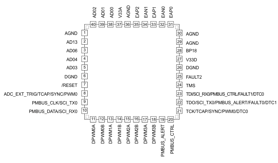
3.2 UCD3138A RMH Package
40 WQFN Package
With Corner Anchors Pin Attributes
Top View

UCD3138A RMH Pin Functions
| PIN NO. | NAME | PRIMARY ASSIGNMENT | ALTERNATE ASSIGNMENT | CONFIGURABLE AS A GPIO? |
|||
|---|---|---|---|---|---|---|---|
| NO. 1 | NO. 2 | NO. 3 | NO. 4 | ||||
| 1 | AGND | Analog ground | |||||
| 2 | AD13 | 12-bit ADC, Ch 13, Connected to comparator E, I-share | |||||
| 3 | AD06 | 12-bit ADC, Ch 6, Connected to comparator F | |||||
| 4 | AD04 | 12-bit ADC, Ch 4, Connected to comparator D | |||||
| 5 | AD03 | 12-bit ADC, Ch 3, Connected to comparator B and C | |||||
| 6 | DGND | Digital ground | |||||
| 7 | RESET | Device Reset Input, active low | |||||
| 8 | ADC_EXT_TRIG | ADC conversion external trigger input | TCAP | SYNC | PWM0 | Yes | |
| 9 | PMBUS_CLK | PMBUS Clock (Open Drain) | SCI_TX0 | Yes | |||
| 10 | PMBUS_DATA | PMBus data (Open Drain) | SCI_RX0 | Yes | |||
| 11 | DPWM0A | DPWM 0A output | Yes | ||||
| 12 | DPWM0B | DPWM 0B output | Yes | ||||
| 13 | DPWM1A | DPWM 1A output | Yes | ||||
| 14 | DPWM1B | DPWM 1B output | Yes | ||||
| 15 | DPWM2A | DPWM 2A output | Yes | ||||
| 16 | DPWM2B | DPWM 2B output | Yes | ||||
| 17 | DWPM3A | DPWM 3A output | Yes | ||||
| 18 | DPWM3B | DPWM 3B output | Yes | ||||
| 19 | PMBUS_ALERT | PMBus Alert (Open Drain) | Yes | ||||
| 20 | PMBUS_CTRL | PMBus Control (Open Drain) | Yes | ||||
| 21 | TCK | JTAG TCK | TCAP | SYNC | PWM0 | DTC0 | Yes |
| 22 | TDO | JTAG TDO | SCI_TX0 | PMBUS_ALERT | FAULT0 | DTC1 | Yes |
| 23 | TDI | JTAG TDI | SCI_RX0 | PMBUS_CTRL | FAULT1 | DTC0 | Yes |
| 24 | TMS | JTAG TMS | Yes | ||||
| 25 | FAULT2 | External fault input 2 | Yes | ||||
| 26 | DGND | Digital ground | |||||
| 27 | V33D | Digital 3.3V core supply | |||||
| 28 | BP18 | 1.8V Bypass | |||||
| 29 | AGND | Substrate analog ground | |||||
| 30 | AGND | Analog ground | |||||
| 31 | EAP0 | Channel 0, differential analog voltage, positive input | |||||
| 32 | EAN0 | Channel 0, differential analog voltage, negative input | |||||
| 33 | EAP1 | Channel 1, differential analog voltage, positive input | |||||
| 34 | EAN1 | Channel 1, differential analog voltage, negative input | |||||
| 35 | EAP2 | Channel 2, differential analog voltage, positive input (Recommended for peak currrent mode control) |
|||||
| 36 | AGND | Analog ground | |||||
| 37 | V33A | Analog 3.3-V supply | |||||
| 38 | AD00 | 12-bit ADC, Ch 0, Connected to current source | |||||
| 39 | AD01 | 12-bit ADC, Ch 1, Connected to current source | |||||
| 40 | AD02 | 12-bit ADC, Ch 2, Connected to comparator A, I-share | |||||
| Corner NA |
Corner anchor pin |
All four anchors should be soldered and tied to GND | |||||
3.3 UCD3138A RJA Package
40 VQFN Package
With Corner Anchors Pin Attributes
Top View

The RJA package has thicker package height compared to the RMH package. There are four corner pins on the RJA package. These features help to improve solder-joint reliability. The corner anchor pins and thermal pad should be soldered for robust mechanical performance and should be tied to the appropriate ground signal.
UCD3138A RJA Pin Functions
| PIN NO. | NAME | PRIMARY ASSIGNMENT | ALTERNATE ASSIGNMENT | CONFIGURABLE AS A GPIO? |
|||
|---|---|---|---|---|---|---|---|
| NO. 1 | NO. 2 | NO. 3 | NO. 4 | ||||
| 1 | AGND | Analog ground | |||||
| 2 | AD13 | 12-bit ADC, Ch 13, Connected to comparator E, I-share | |||||
| 3 | AD06 | 12-bit ADC, Ch 6, Connected to comparator F | |||||
| 4 | AD04 | 12-bit ADC, Ch 4, Connected to comparator D | |||||
| 5 | AD03 | 12-bit ADC, Ch 3, Connected to comparator B and C | |||||
| 6 | DGND | Digital ground | |||||
| 7 | RESET | Device Reset Input, active low | |||||
| 8 | ADC_EXT_TRIG | ADC conversion external trigger input | TCAP | SYNC | PWM0 | Yes | |
| 9 | PMBUS_CLK | PMBUS Clock (Open Drain) | SCI_TX0 | Yes | |||
| 10 | PMBUS_DATA | PMBus data (Open Drain) | SCI_RX0 | Yes | |||
| 11 | DPWM0A | DPWM 0A output | Yes | ||||
| 12 | DPWM0B | DPWM 0B output | Yes | ||||
| 13 | DPWM1A | DPWM 1A output | Yes | ||||
| 14 | DPWM1B | DPWM 1B output | Yes | ||||
| 15 | DPWM2A | DPWM 2A output | Yes | ||||
| 16 | DPWM2B | DPWM 2B output | Yes | ||||
| 17 | DWPM3A | DPWM 3A output | Yes | ||||
| 18 | DPWM3B | DPWM 3B output | Yes | ||||
| 19 | PMBUS_ALERT | PMBus Alert (Open Drain) | Yes | ||||
| 20 | PMBUS_CTRL | PMBus Control (Open Drain) | Yes | ||||
| 21 | TCK | JTAG TCK | TCAP | SYNC | PWM0 | DTC0 | Yes |
| 22 | TDO | JTAG TDO | SCI_TX0 | PMBUS_ALERT | FAULT0 | DTC1 | Yes |
| 23 | TDI | JTAG TDI | SCI_RX0 | PMBUS_CTRL | FAULT1 | DTC0 | Yes |
| 24 | TMS | JTAG TMS | Yes | ||||
| 25 | FAULT2 | External fault input 2 | Yes | ||||
| 26 | DGND | Digital ground | |||||
| 27 | V33D | Digital 3.3V core supply | |||||
| 28 | BP18 | 1.8V Bypass | |||||
| 29 | AGND | Substrate analog ground | |||||
| 30 | AGND | Analog ground | |||||
| 31 | EAP0 | Channel 0, differential analog voltage, positive input | |||||
| 32 | EAN0 | Channel 0, differential analog voltage, negative input | |||||
| 33 | EAP1 | Channel 1, differential analog voltage, positive input | |||||
| 34 | EAN1 | Channel 1, differential analog voltage, negative input | |||||
| 35 | EAP2 | Channel 2, differential analog voltage, positive input (Recommended for peak currrent mode control) |
|||||
| 36 | AGND | Analog ground | |||||
| 37 | V33A | Analog 3.3-V supply | |||||
| 38 | AD00 | 12-bit ADC, Ch 0, Connected to current source | |||||
| 39 | AD01 | 12-bit ADC, Ch 1, Connected to current source | |||||
| 40 | AD02 | 12-bit ADC, Ch 2, Connected to comparator A, I-share | |||||
| Corner NA |
Corner anchor pin |
All four anchors should be soldered and tied to GND | |||||