SLVSCS1B March 2015 – May 2015 UCD7138
PRODUCTION DATA.
- 1 Features
- 2 Applications
- 3 Description
- 4 Simplified Schematic
- 5 Revision History
- 6 Pin Configuration and Functions
- 7 Specifications
- 8 Detailed Description
- 9 Application and Implementation
- 10Power Supply Recommendations
- 11Layout
- 12Device and Documentation Support
- 13Mechanical, Packaging, and Orderable Information
Package Options
Mechanical Data (Package|Pins)
- DRS|6
Thermal pad, mechanical data (Package|Pins)
Orderable Information
1 Features
- Low-Side Gate Driver With Body-Diode Conduction Sensing
- Gate Turnoff Edge Body-Diode Conduction Reporting
- Gate Turnon Edge Delay Optimization
- Works Together With the Dead-Time Compensation (DTC) Module in the UCD3138A Family of Digital Power Controllers:
- Automatic or Manual Dead-Time Adjustment of Gate Turnon and Turnoff Edges
- Negative Current Protection
- -150-mV Body-Diode Conduction Sensing Threshold
- Able to Sense Body Diode Conduction Times as Low as 10 ns
- 4-A Peak-Source and 6-A Peak-Sink Drive Current
- Fast Propagation Delays (14-ns Typical)
- Fast Rise and Fall Times (5-ns Typical)
- Up to 2-MHz Operating Frequency
- 4.5-V to 18-V Supply Range
- Rail-to-Rail Drive Capability
- VCC Undervoltage Lockout (UVLO)
- 6-Pin 3-mm × 3-mm WSON-6 Package
2 Applications
- LLC Converters
- Hard Switching Full-Bridge Converters
- Digital Power-Control Applications
3 Description
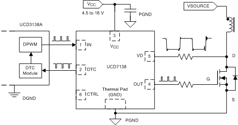
The UCD7138 device is a 4-A and 6-A single-channel MOSFET driver with body-diode conduction sensing and reporting and is a high performance driver that allows the Texas Instruments UCD3138A digital PWM controller to achieve advanced synchronous-rectification (SR) control. The device contains a high-speed gate driver, a body-diode conduction-sensing circuit, and a turnon delay optimization circuit. The device is suitable for high-power, high-efficiency isolated converter applications where SR dead-time optimization is desired.
The UCD7138 device offers asymmetrical rail-to-rail 4-A source and 6-A sink peak-current drive capability. The short propagation delay and fast rise and fall time allows efficient operation at high frequencies. An internal high-speed comparator with a –150-mV threshold detects the body-diode conduction and reports the information to the UCD3138A digital-power controller. The UCD7138 device is capable of sensing body-diode conduction time as low as 10 ns. The SR turnon edge is optimized by the UCD7138 device. The SR turnoff edge is optimized by the UCD3138A digital-power controller which analyzes the body-diode conduction information reported by the UCD7138 DTC pin.
The benefits of the chipset include maximizing system efficiency by minimizing body-diode conduction time, robust and fast negative-current protection, and a simple interface.
Device Information(1)
| PART NUMBER | PACKAGE | BODY SIZE (NOM) |
|---|---|---|
| UCD7138 | WSON (6) | 3.00 mm × 3.00 mm |
- For all available packages, see the orderable addendum at the end of the datasheet.
4 Simplified Schematic

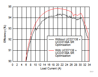
Power Savings for a 340-W LLC Application
