SLVSDD4C September 2016 – March 2020 UCD90160A
PRODUCTION DATA.
- 1 Features
- 2 Applications
- 3 Description
- 4 Revision History
- 5 Pin Configuration and Functions
- 6 Specifications
-
7 Detailed Description
- 7.1 Overview
- 7.2 Functional Block Diagram
- 7.3 Feature Description
- 7.4
Device Functional Modes
- 7.4.1 Power Supply Sequencing
- 7.4.2 Pin-Selected Rail States
- 7.4.3 Voltage Monitoring
- 7.4.4 Fault Responses and Alert Processing
- 7.4.5 Shut Down All Rails and Sequence On (Resequence)
- 7.4.6 GPIOs
- 7.4.7 GPO Control
- 7.4.8 GPO Dependencies
- 7.4.9 GPI Special Functions
- 7.4.10 Power Supply Enables
- 7.4.11 Cascading Multiple Devices
- 7.4.12 PWM Outputs
- 7.4.13 Programmable Multiphase PWMs
- 7.4.14 Margining
- 7.4.15 System Reset Signal
- 7.4.16 Watch Dog Timer
- 7.4.17 Run Time Clock
- 7.4.18 Data and Error Logging to Flash Memory
- 7.4.19 Brownout Function
- 7.4.20 PMBus Address Selection
- 7.4.21 Device Reset
- 7.5 Programming
- 8 Application and Implementation
- 9 Power Supply Recommendations
- 10Layout
- 11Device and Documentation Support
- 12Mechanical, Packaging, and Orderable Information
Package Options
Mechanical Data (Package|Pins)
- RGC|64
Thermal pad, mechanical data (Package|Pins)
- RGC|64
Orderable Information
7.5.1 Device Configuration and Programming
From the factory, the device contains the sequencing and monitoring firmware. It is also configured so that all GPOs are high-impedance (except for FPWM/GPIO pins 17 to 24, which are driven low), with no sequencing or fault-response operation. See Configuration Programming of UCD Devices, available from the Documentation & Help Center that can be selected from the Fusion Digital Power Designer software Help menu, for full UCD90160A configuration details.
After the user has designed a configuration file using Fusion GUI, there are three general device-configuration programming options:
- Devices can be programmed in-circuit by a host microcontroller using PMBus commands over I2C (see the UCD90xxx Sequencer and System Health Controller PMBus Command Reference).
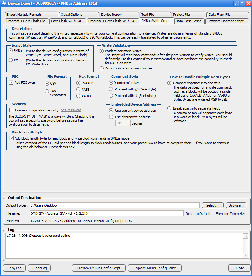
Each parameter write replaces the data in the associated memory (RAM) location. After all the required configuration data has been sent to the device, it is transferred to the associated nonvolatile memory (data flash) by issuing a special command, STORE_DEFAULT_ALL. This method is how the Fusion Digital Power Designer software normally reads and writes a device configuration. This method may cause unexpected behaviors on GPIO pins which can disable rails that provide power to device. It is not recommended for production programming. - The Fusion Digital Power Designer software (Figure 30) can create a PMBus or I2C command script file that can be used by the I2C master to configure the device. This method may cause unexpected behaviors on GPIO pins which can disable rails that provide power to device. It is not recommended for production programming.
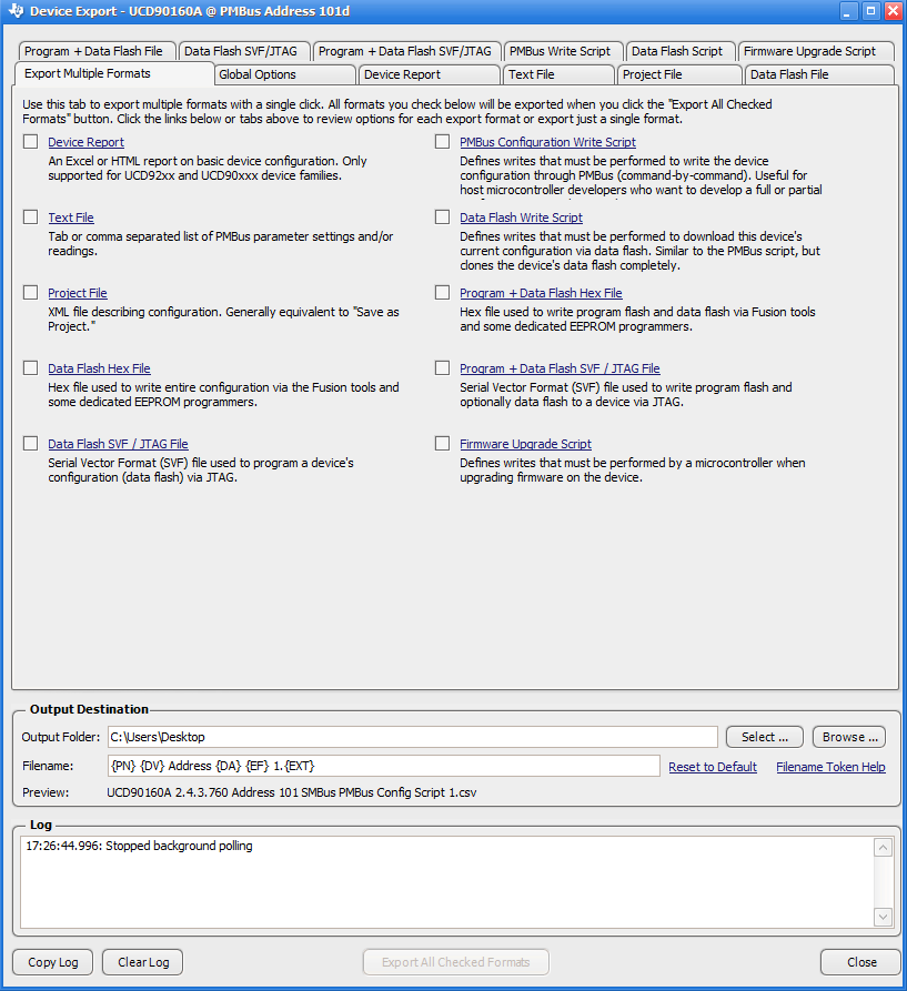
- Another in-circuit programming option is for the Fusion Digital Power Designer software to create a data flash image from the configuration file (Figure 31). The configuration files can be exported in Intel Hex, data flash script, Serial Vector Format (SVF) and S-record. The image file can be downloaded into the device using I2C or JTAG. The Fusion Digital Power Designer software tools can be used on-board if the Fusion Digital Power Designer software can gain ownership of the target board I2C bus. It is recommended to use Intel Hex file or data flash script file for production programming because the GPIOs are under controlled states.
 Figure 30. Fusion GUI PMBus Configuration Script Export Tool
  Figure 31. Fusion GUI Device Configuration Export Tool
 Devices can be programmed off-board using the Fusion GUI tools or a dedicated device programmer. For small runs, a ZIF socketed board with an I2C header can be used with the standard Fusion GUI or manufacturing GUI. Use the UCD90SEQ64EVM-650: 64-Pin Sequencer Development Board. The Fusion Digital Power Designer software can also create a data flash file that can then be loaded into the UCD90160A device using a dedicated device programmer.
The UCD90160A must be powered in order to configure it using an I2C or PMBus interface. The PMBus clock and data pins must be accessible and must be pulled high to the same VDD supply that powers the device, with pullup resistors between 1 kΩ and 2 kΩ. Do not introduce additional bus capacitance (< 100 pF). Write the user configuration to data flash using a gang programmer via JTAG or I2C interface before the device is installed in a circuit. To use the I2C interface, the clock and data lines must be multiplexed or the device addresses must be assigned by socket. The Fusion Digital Power Designer software tools can be used for socket addressing. Pre-programming can also be done using a single device test fixture.
Table 13. Configuration Options
| DATA FLASH VIA JTAG | DATA FLASH VIA I2C(Recommend) | PMBus COMMANDS VIA I2C | |
|---|---|---|---|
| Off-Board Configuration | Data Flash Export (.svf type file) | Data Flash Export (.srec or hex, data flash script type file) | System file/Project file I2C/PMBus script |
| Dedicated programmer | Fusion tools (with exclusive bus access via USB to I2C adapter) | Fusion tools (with exclusive bus access via USB to I2C adapter) | |
| On-Board Configuration | Data flash export | Fusion tools (with exclusive bus access via USB to I2C adapter) | Fusion tools (with exclusive bus access via USB to I2C adapter) |
| IC |
The advantages of off-board configuration include:
- Does not require access to device I2C bus on board.
- Once soldered on board, full board power is available without further configuration.
- Can be partially reconfigured once the device is mounted.