SLES275A January 2015 – December 2017 VSP5324-Q1
PRODUCTION DATA.
- 1 Features
- 2 Applications
- 3 Description
- 4 Revision History
- 5 Pin Configuration and Functions
-
6 Specifications
- 6.1 Absolute Maximum Ratings
- 6.2 ESD Ratings
- 6.3 Recommended Operating Conditions
- 6.4 Thermal Information
- 6.5 Electrical Characteristics: Dynamic Performance
- 6.6 Electrical Characteristics: General
- 6.7 Electrical Characteristics: Digital
- 6.8 Timing Requirements
- 6.9 LVDS Timing at Different Sampling Frequencies (One-Lane Interface, 12x Serialization)
- 6.10 LVDS Timing at Different Sampling Frequencies (Two-Lane Interface, 6x Serialization)
- 6.11 Serial Interface Timing Requirements
- 6.12 Typical Characteristics
-
7 Detailed Description
- 7.1 Overview
- 7.2 Functional Block Diagrams
- 7.3 Feature Description
- 7.4 Device Functional Modes
- 7.5 Programming
- 7.6
Register Maps
- 7.6.1
Serial Registers
- 7.6.1.1 Register 00h (offset = 00h) [reset = 0]
- 7.6.1.2 Register 01h (offset = 01h) [reset = 0]
- 7.6.1.3 Register 02h (offset = 02h) [reset = 0]
- 7.6.1.4 Register 0Ah (offset = 0Ah) [reset = 0]
- 7.6.1.5 Register 0Fh (offset = 0Fh) [reset = 0]
- 7.6.1.6 Register 14h (offset = 14h) [reset = 0]
- 7.6.1.7 Register 1Ch (offset = 1Ch) [reset = 0]
- 7.6.1.8 Register 23h (offset = 23h) [reset = 0]
- 7.6.1.9 Register 24h (offset = 24h) [reset = 0]
- 7.6.1.10 Register 25h (offset = 25h) [reset = 0]
- 7.6.1.11 Register 26h (offset = 26h) [reset = 0]
- 7.6.1.12 Register 27h (offset = 27h) [reset = 0]
- 7.6.1.13 Register 28h (offset = 28h) [reset = 0]
- 7.6.1.14 Register 29h (offset = 29h) [reset = 0]
- 7.6.1.15 Register 2Ah (offset = 2Ah) [reset = 0]
- 7.6.1.16 Register 2Bh (offset = 2Bh) [reset = 0]
- 7.6.1.17 Register 2Eh (offset = 2Eh) [reset = 0]
- 7.6.1.18 Register 30h (offset = 30h) [reset = 0]
- 7.6.1.19 Register 33h (offset = 33h) [reset = 0]
- 7.6.1.20 Register 35h (offset = 35h) [reset = 0]
- 7.6.1.21 Register 38h (offset = 38h) [reset = 0x0000]
- 7.6.1.22 Register 42h (offset = 42h) [reset = 0]
- 7.6.1.23 Register 45h (offset = 45h) [reset = 0]
- 7.6.1.24 Register 46h (offset = 46h) [reset = 0]
- 7.6.1.25 Register 50h (offset = 50h) [reset = 0]
- 7.6.1.26 Register 51h (offset = 51h) [reset = 0]
- 7.6.1.27 Register 53h (offset = 53h) [reset = 0]
- 7.6.1.28 Register 54h (offset = ) [reset = 0]
- 7.6.1.29 Register 55h (offset = 55h) [reset = 0]
- 7.6.1.30 Register F0h (offset = F0h) [reset = 0]
- 7.6.1
Serial Registers
- 8 Application and Implementation
- 9 Power Supply Recommendations
- 10Layout
- 11Device and Documentation Support
- 12Mechanical, Packaging, and Orderable Information
Package Options
Mechanical Data (Package|Pins)
- RGC|64
Thermal pad, mechanical data (Package|Pins)
- RGC|64
Orderable Information
10 Layout
10.1 Layout Guidelines
10.1.1 General Guidelines
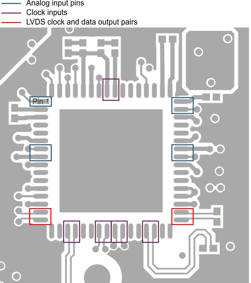
The following list includes general layout guidelines. Refer to Figure 86 as needed.
- Route the clock input as a differential pair when a differential clock input is used.
- When single ended inputs are used, place 100-nF capacitors close to the pins on the INx_M inputs to ensure that the reference rail is stable. When differential inputs are used, the inputs must be routed as differential pairs.
- Route the LVDS clock and data output pairs with 100-Ω differential impedance and length matched as per the sampling frequency.
10.1.2 Grounding
A single ground plane is sufficient to provide good performance, provided that the analog, digital, and clock sections of the board are cleanly partitioned.
10.1.3 Supply Decoupling
Minimal external decoupling can be used without loss in performance because the VSP5324-Q1 device already includes internal decoupling. Note that decoupling capacitors can help filter external power-supply noise, thus the optimum number of capacitors depends on the actual application. The decoupling capacitors should be placed very close to the converter supply pins.
10.1.4 Exposed Pad
In addition to providing a path for heat dissipation, the pad is also electrically connected to the digital ground internally. Therefore, soldering the exposed pad to the ground plane is necessary to achieve the best thermal and electrical performance. For detailed information, see application notes QFN Layout Guidelines and QFN/SON PCB Attachment.
10.2 Layout Example
