JAJSFC6C May   2015  – April 2018 ADS52J90

PRODUCTION DATA.  

  1. 特長
  2. アプリケーション
  3. 概要
    1.     概略回路図
  4. 改訂履歴
  5. 概要(続き)
  6. Pin Configuration and Functions
    1.     Pin Functions
  7. Specifications
    1. 7.1  Absolute Maximum Ratings
    2. 7.2  ESD Ratings
    3. 7.3  Recommended Operating Conditions
    4. 7.4  Thermal Information
    5. 7.5  Electrical Characteristics
    6. 7.6  Digital Characteristics
    7. 7.7  Timing Requirements: Signal Chain
    8. 7.8  Timing Requirements: JESD Interface
    9. 7.9  Timing Requirements: Serial Interface
    10. 7.10 Typical Characteristics
    11. 7.11 Typical Characteristics: JESD Interface
    12. 7.12 Typical Characteristics: Contour Plots
  8. Detailed Description
    1. 8.1 Overview
    2. 8.2 Functional Block Diagrams
    3. 8.3 Feature Description
      1. 8.3.1  Connection of the External Inputs to the Input Pins
      2. 8.3.2  Input Multiplexer and Sampler
      3. 8.3.3  Analog-to-Digital Converter (ADC)
      4. 8.3.4  Device Synchronization Using TX_TRIG
      5. 8.3.5  Digital Processing
        1. 8.3.5.1 Digital Offset
          1. 8.3.5.1.1 Manual Offset Correction
          2. 8.3.5.1.2 Auto Offset Correction Mode (Offset Correction using a Built-In Offset Calculation Function)
          3. 8.3.5.1.3 Digital Averaging
          4. 8.3.5.1.4 Digital Gain
          5. 8.3.5.1.5 Digital HPF
      6. 8.3.6  Data Formatting
      7. 8.3.7  Serializer and LVDS Interface
      8. 8.3.8  LVDS Buffers
      9. 8.3.9  JESD204B Interface
        1. 8.3.9.1 Overview
        2. 8.3.9.2 Link Configuration
        3. 8.3.9.3 JESD Version and Subclass
        4. 8.3.9.4 Transport Layer
          1. 8.3.9.4.1 User Data Format
          2. 8.3.9.4.2 Transport Layer Test Patterns
        5. 8.3.9.5 Scrambler
        6. 8.3.9.6 Data Link Layer
          1. 8.3.9.6.1 Code Group Synchronization (CGS)
          2. 8.3.9.6.2 Initial Lane Alignment (ILA)
          3. 8.3.9.6.3 Lane and Frame Alignment Monitoring
          4. 8.3.9.6.4 Link Layer Test Modes
        7. 8.3.9.7 Deterministic Latency
          1. 8.3.9.7.1 Synchronization Using SYNC~ and SYSREF
          2. 8.3.9.7.2 Latency
          3. 8.3.9.7.3 Multiframe Size
        8. 8.3.9.8 JESD Physical Layer
          1. 8.3.9.8.1 CML Buffer
          2. 8.3.9.8.2 Jitter Considerations
      10. 8.3.10 Interfacing SYNC~ and SYSREF Between the FPGA and ADCs
      11. 8.3.11 Clock Input
      12. 8.3.12 Analog Input and Driving Circuit
        1. 8.3.12.1 Signal Input
    4. 8.4 Device Functional Modes
      1. 8.4.1 Input Modes
      2. 8.4.2 ADC Resolution Modes
      3. 8.4.3 LVDS and JESD Interface Modes
      4. 8.4.4 LVDS Serialization and Output Data Rate Modes
      5. 8.4.5 Power Modes
      6. 8.4.6 LVDS Test Pattern Mode
    5. 8.5 Programming
      1. 8.5.1 Serial Peripheral Interface (SPI) Operation
        1. 8.5.1.1 Serial Register Write Description
        2. 8.5.1.2 Register Readout
  9. Application and Implementation
    1. 9.1 Application Information
    2. 9.2 Typical Application
      1. 9.2.1 Design Requirements
      2. 9.2.2 Detailed Design Procedure
        1. 9.2.2.1 Designing with the 16-Input Mode
        2. 9.2.2.2 Designing with the 32-Input Mode
        3. 9.2.2.3 Designing with the 8-Input Mode
      3. 9.2.3 Application Curves
    3. 9.3 Do's and Don'ts
  10. 10Power Supply Recommendations
    1. 10.1 Power Sequencing and Initialization
  11. 11Layout
    1. 11.1 Power Supply, Grounding, and Bypassing
    2. 11.2 Layout Guidelines
    3. 11.3 Layout Example
  12. 12Register Map
    1. 12.1 ADC Registers
      1. 12.1.1 Description of Registers
        1. 12.1.1.1  Register 0h (address = 0h)
          1. Table 47. Register 0h Field Descriptions
        2. 12.1.1.2  Register 1h (address = 1h)
          1. Table 48. Register 1h Field Descriptions
        3. 12.1.1.3  Register 2h (address = 2h)
          1. Table 51. Register 2h Field Descriptions
        4. 12.1.1.4  Register 3h (address = 3h)
          1. Table 53. Register 3h Field Descriptions
        5. 12.1.1.5  Register 4h (address = 4h)
          1. Table 54. Register 4h Field Descriptions
        6. 12.1.1.6  Register 5h (address = 5h)
          1. Table 55. Register 5h Field Descriptions
        7. 12.1.1.7  Register 7h (address = 7h)
          1. Table 56. Register 7h Field Descriptions
        8. 12.1.1.8  Register 8h (address = 8h)
          1. Table 57. Register 8h Field Descriptions
        9. 12.1.1.9  Register Ah (address = Ah)
          1. Table 58. Register Ah Field Descriptions
        10. 12.1.1.10 Register Bh (address = Bh)
          1. Table 59. Register Bh Field Descriptions
        11. 12.1.1.11 Register Dh (address = Dh)
          1. Table 60. Register Dh Field Descriptions
        12. 12.1.1.12 Register Eh (address = Eh)
          1. Table 61. Register Eh Field Descriptions
        13. 12.1.1.13 Register Fh (address = Fh)
          1. Table 62. Register Fh Field Descriptions
        14. 12.1.1.14 Register 10h (address = 10h)
          1. Table 63. Register 10h Field Descriptions
        15. 12.1.1.15 Register 11h (address = 11h)
          1. Table 64. Register 11h Field Descriptions
        16. 12.1.1.16 Register 12h (address = 12h)
          1. Table 65. Register 12h Field Descriptions
        17. 12.1.1.17 Register 13h (address = 13h)
          1. Table 66. Register 13h Field Descriptions
        18. 12.1.1.18 Register 14h (address = 14h)
          1. Table 67. Register 14h Field Descriptions
        19. 12.1.1.19 Register 15h (address = 15h)
          1. Table 68. Register 15h Field Descriptions
        20. 12.1.1.20 Register 17h (address = 17h)
          1. Table 69. Register 17h Field Descriptions
        21. 12.1.1.21 Register 18h (address = 18h)
          1. Table 70. Register 18h Field Descriptions
        22. 12.1.1.22 Register 19h (address = 19h)
          1. Table 71. Register 19h Field Descriptions
        23. 12.1.1.23 Register 1Ah (address = 1Ah)
          1. Table 72. Register 1Ah Field Descriptions
        24. 12.1.1.24 Register 1Bh (address = 1Bh)
          1. Table 73. Register 1Bh Field Descriptions
        25. 12.1.1.25 Register 1Ch (address = 1Ch)
          1. Table 74. Register 1Ch Field Descriptions
        26. 12.1.1.26 Register 1Dh (address = 1Dh)
          1. Table 75. Register 1Dh Field Descriptions
        27. 12.1.1.27 Register 1Eh (address = 1Eh)
          1. Table 76. Register 1Eh Field Descriptions
        28. 12.1.1.28 Register 1Fh (address = 1Fh)
          1. Table 77. Register 1Fh Field Descriptions
        29. 12.1.1.29 Register 20h (address = 20h)
          1. Table 78. Register 20h Field Descriptions
        30. 12.1.1.30 Register 21h (offset = 21h)
          1. Table 79. Register 21h Field Descriptions
        31. 12.1.1.31 Register 23h (register = 23h)
          1. Table 80. Register 23h Field Descriptions
        32. 12.1.1.32 Register 24h (address = 24h)
          1. Table 81. Register 24h Field Descriptions
        33. 12.1.1.33 Register 25h (address = 25h)
          1. Table 82. Register 25h Field Descriptions
        34. 12.1.1.34 Register 26h (address = 26h)
          1. Table 83. Register 26h Field Descriptions
        35. 12.1.1.35 Register 27h (address = 27h)
          1. Table 84. Register 27h Field Descriptions
        36. 12.1.1.36 Register 28h (address = 28h)
          1. Table 85. Register 28h Field Descriptions
        37. 12.1.1.37 Register 29h (address = 29h)
          1. Table 86. Register 29h Field Descriptions
        38. 12.1.1.38 Register 2Ah (address = 2Ah)
          1. Table 87. Register 2Ah Field Descriptions
        39. 12.1.1.39 Register 2Bh (address = 2Bh)
          1. Table 88. Register 2Bh Field Descriptions
        40. 12.1.1.40 Register 2Ch (address = 2Ch)
          1. Table 89. Register 2Ch Field Descriptions
        41. 12.1.1.41 Register 2Dh (address = 2Dh)
          1. Table 90. Register 2Dh Field Descriptions
        42. 12.1.1.42 Register 2Fh (address = 2Fh)
          1. Table 91. Register 2Fh Field Descriptions
        43. 12.1.1.43 Register 30h (address = 30h)
          1. Table 92. Register 30h Field Descriptions
        44. 12.1.1.44 Register 31h (address = 31h)
          1. Table 93. Register 31h Field Descriptions
        45. 12.1.1.45 Register 32h (address = 32h)
          1. Table 94. Register 32h Field Descriptions
        46. 12.1.1.46 Register 33h (address = 33h)
          1. Table 95. Register 33h Field Descriptions
        47. 12.1.1.47 Register 34h (address = 34h)
          1. Table 96. Register 34h Field Descriptions
        48. 12.1.1.48 Register 35h (address = 35h)
          1. Table 97. Register 35h Field Descriptions
        49. 12.1.1.49 Register 36h (address = 36h)
          1. Table 98. Register 36h Field Descriptions
        50. 12.1.1.50 Register 37h (address = 37h)
          1. Table 99. Register 37h Field Descriptions
        51. 12.1.1.51 Register 38h (address = 38h)
          1. Table 100. Register 38h Field Descriptions
        52. 12.1.1.52 Register 39h (address = 39h)
          1. Table 101. Register 39h Field Descriptions
        53. 12.1.1.53 Register 3Bh (address = 3Bh)
          1. Table 102. Register 3Bh Field Descriptions
        54. 12.1.1.54 Register 3Ch (address = 3Ch)
          1. Table 103. Register 3Ch Field Descriptions
        55. 12.1.1.55 Register 43h (address = 43h)
          1. Table 104. Register 43h Field Descriptions
    2. 12.2 JESD Serial Interface Registers
      1. 12.2.1 Description of JESD Serial Interface Registers
        1. 12.2.1.1  Register 70 (address = 46h)
          1. Table 106. Register 70 Field Descriptions
        2. 12.2.1.2  Register 73 (address = 49h)
          1. Table 107. Register 73 Field Descriptions
        3. 12.2.1.3  Register 74 (address = 4Ah)
          1. Table 108. Register 74 Field Descriptions
        4. 12.2.1.4  Register 75 (address = 4Bh)
          1. Table 109. Register 75 Field Descriptions
        5. 12.2.1.5  Register 77 (address = 4Dh)
          1. Table 110. Register 77 Field Descriptions
        6. 12.2.1.6  Register 80 (address = 50h)
          1. Table 111. Register 80 Field Descriptions
        7. 12.2.1.7  Register 81 (address = 51h)
          1. Table 112. Register 81 Field Descriptions
        8. 12.2.1.8  Register 82 (address = 52h)
          1. Table 113. Register 82 Field Descriptions
        9. 12.2.1.9  Register 83 (address = 53h)
          1. Table 114. Register 83 Field Descriptions
        10. 12.2.1.10 Register 85 (address = 55h)
          1. Table 115. Register 85 Field Descriptions
        11. 12.2.1.11 Register 115 (address = 73h)
          1. Table 116. Register 115 Field Descriptions
        12. 12.2.1.12 Register 116 (address = 74h)
          1. Table 117. Register 116 Field Descriptions
        13. 12.2.1.13 Register 117 (address = 75h)
          1. Table 118. Register 117 Field Descriptions
        14. 12.2.1.14 Register 118 (address = 76h)
          1. Table 119. Register 118 Field Descriptions
        15. 12.2.1.15 Register 119 (address = 77h)
          1. Table 120. Register 119 Field Descriptions
        16. 12.2.1.16 Register 120 (address = 78h)
          1. Table 121. Register 120 Field Descriptions
        17. 12.2.1.17 Register 134 (address = 86h)
          1. Table 122. Register 134 Field Descriptions
        18. 12.2.1.18 Register 135 (address = 87h)
          1. Table 123. Register 135 Field Descriptions
        19. 12.2.1.19 Register 136 (address = 88h)
          1. Table 124. Register 136 Field Descriptions
        20. 12.2.1.20 Register 137 (address = 89h)
          1. Table 125. Register 137 Field Descriptions
        21. 12.2.1.21 Register 138 (address = 8Ah)
          1. Table 126. Register 138 Field Descriptions
  13. 13デバイスおよびドキュメントのサポート
    1. 13.1 ドキュメントのサポート
      1. 13.1.1 関連資料
    2. 13.2 コミュニティ・リソース
    3. 13.3 商標
    4. 13.4 静電気放電に関する注意事項
    5. 13.5 Glossary
  14. 14メカニカル、パッケージ、および注文情報

パッケージ・オプション

メカニカル・データ(パッケージ|ピン)
  • ZZE|198
サーマルパッド・メカニカル・データ
発注情報

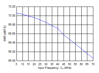
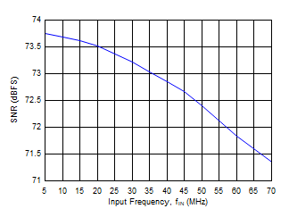
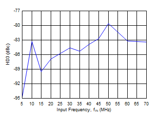
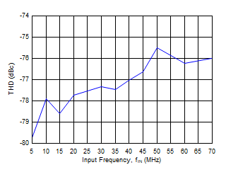
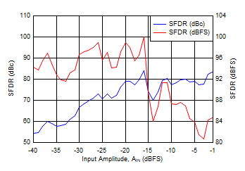
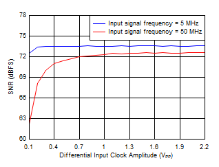
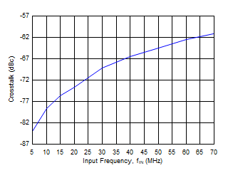
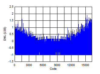
Typical Characteristics

At 25°C, AVDD_IP8 = DVDD_1P8 = 1.8 V, and DVDD_1P2 = 1.2 V, unless otherwise noted. All LVDS outputs are active with 100-Ω differential terminations and a 4-pF load capacitor from each LVDS output pin to ground. A –1-dBFS input signal at 5 MHz is applied to the input channel under test. SNR is computed by ignoring the power contained in the first nine harmonic bins, the fS / 2 and fS / 4 frequency bins as well as the bins corresponding to the intermodulation frequencies between the input and the clock. A LVPECL clock is used as the clock source.
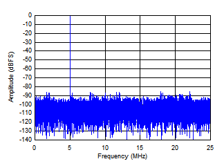
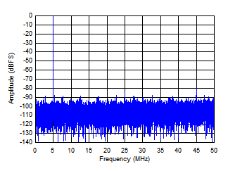
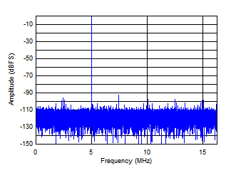
ADS52J90 D002_sbas623.gif
fIN = 5 MHz, fC = 100 MSPS, SNR = 61.5 dBFS,
SFDR = 81.9 dBc, HD2 = –86.5 dBc, HD3 = –93.9 dBc
Figure 2. FFT of 10-Bit, 32-Input Mode
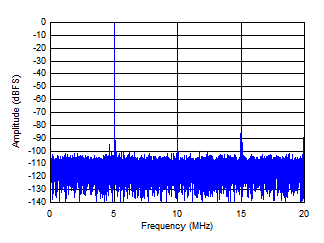
ADS52J90 D004_sbas623.gif
fIN = 5 MHz, fC = 100 MSPS, SNR = 61.3 dBFS,
SFDR = 70.8 dBc, HD2 = –94.2 dBc, HD3 = –80.1 dBc
Figure 4. FFT of 10-Bit, 8-Input Mode
ADS52J90 D006_sbas623.gif
fIN = 5 MHz, fC = 80 MSPS, SNR = 70.2 dBFS, SFDR = 75.4 dBc, HD2 = –109.8 dBc, HD3 = –86.1 dBc
Figure 6. FFT of 12-Bit, 16-Input Mode
ADS52J90 D008_sbas623.gif
fIN = 5 MHz, fC = 65 MSPS, SNR = 73.4 dBFS, SFDR = 80.2 dBc, HD2 = –88.7 dBc, HD3 = –93.9 dBc
Figure 8. FFT of 14-Bit, 16-Input Mode
ADS52J90 D010_sbas623.gif
fSAMP = 100 MSPS
Figure 10. Signal-to-Noise Ratio vs fIN in
10-Bit, 16-Input Mode
ADS52J90 D012_sbas623.gif
fSAMP = 40 MSPS
Figure 12. Signal-to-Noise Ratio vs fIN in
12-Bit, 32-Input Mode
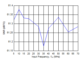
ADS52J90 D014_sbas623.gif
fSAMP = 32.5 MSPS
Figure 14. Signal-to-Noise Ratio vs fIN in
14-Bit, 32-Input Mode
ADS52J90 D016_sbas623.gif
100-MSPS conversion clock
Figure 16. Third-Order Harmonic Distortion vs fIN
ADS52J90 D018_sbas623.gif
100-MSPS conversion clock
Figure 18. Total Harmonic Distortion vs fIN
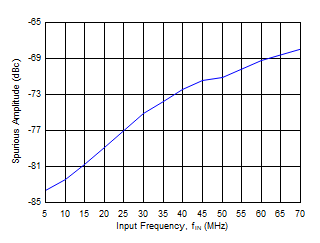
ADS52J90 D020_sbas623.gif
fSAMP = 100 MSPS
Figure 20. Input-Clock Intermodulation Spur at (fS / 2 ± fIN) vs fIN in 16-Input Mode
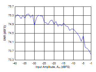
ADS52J90 D022_sbas623.gif
16-input mode, 14-bit resolution, fSAMP = 65 MSPS
Figure 22. Signal-to-Noise Ratio vs AIN
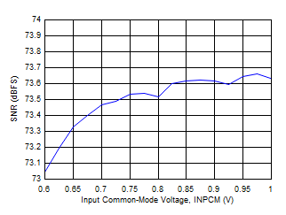
ADS52J90 D024_sbas623.gif
16-input mode, 14-bit resolution, fSAMP = 65 MSPS
Figure 24. Signal-to-Noise Ratio vs
Input Common-Mode Voltage (INPCM)
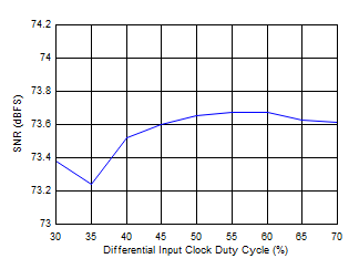
ADS52J90 D026_sbas623.gif
16-input mode, 14-bit resolution, fSAMP = 65 MSPS
space
space
Figure 26. Signal-to-Noise Ratio vs Differential Input
Clock Duty Cycle
ADS52J90 D028_sbas623.gif
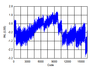
32-input mode, 14-bit resolution, fSAMP = 32.5 MSPS
Figure 28. Integral Nonlinearity
ADS52J90 D030_sbas623.gif
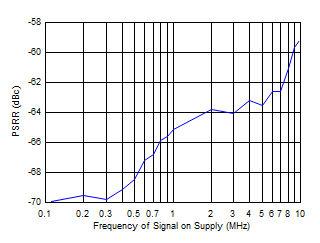
32-input mode, 14-bit resolution, fSAMP = 32.5 MSPS, 100-mVPP tone on supply
Figure 30. Power-Supply Rejection Ratio vs
Frequency of Signal on Supply
ADS52J90 D032_sbas623.gif
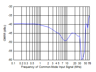
32-input mode, 14-bit resolution, fSAMP = 32.5 MSPS, 50-mVPP common-mode tone applied at the inputs, output tone referred to the input tone
Figure 32. Common-Mode Rejection Ratio vs
Frequency of Common-Mode Input Signal
ADS52J90 D034_sbas623.gif
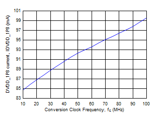
32-input mode, 10-bit resolution
Figure 34. DVDD_1P8 Current vs
Conversion Clock Frequency
ADS52J90 D036_sbas623.gif
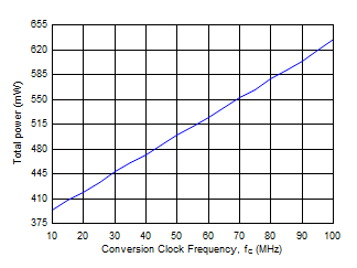
32-input mode, 10-bit resolution
Figure 36. Total Power vs Conversion Clock Frequency
ADS52J90 D046_sbas623.gif
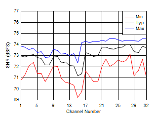
Statistical values taken over 100 devices in 14-bit, 32-input mode at fSAMP = 32.5 MSPS
Figure 38. Signal-to-Noise Ratio Histogram
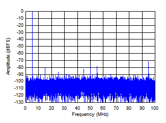
ADS52J90 D003_sbas623.gif
fIN = 5 MHz, fC = 100 MSPS, SNR = 61.6 dBFS,
SFDR = 78.7 dBc, HD2 = –97.6 dBc, HD3 = –92.2 dBc
Figure 3. FFT of 10-Bit, 16-Input Mode
ADS52J90 D005_sbas623.gif
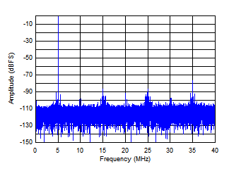
fIN = 5 MHz, fC = 80 MSPS, SNR = 69.9 dBFS, SFDR = 82.6 dBc, HD2 = –82.6 dBc, HD3 = –88.9 dBc
Figure 5. FFT of 12-Bit, 32-Input Mode
ADS52J90 D007_sbas623.gif
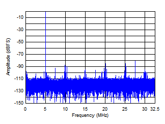
fIN = 5 MHz, fC = 65 MSPS, SNR = 73.7 dBFS, SFDR = 91.8 dBc, HD2 = –96.6 dBc, HD3 = –97.2 dBc
Figure 7. FFT of 14-Bit, 32-Input Mode
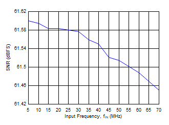
ADS52J90 D009_sbas623.gif
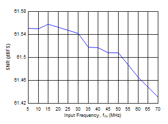
fSAMP = 50 MSPS
Figure 9. Signal-to-Noise Ratio vs fIN in
10-Bit, 32-Input Mode
ADS52J90 D011_sbas623.gif
fSAMP = 200 MSPS
Figure 11. Signal-to-Noise Ratio vs fIN in
10-Bit, 8-Input Mode
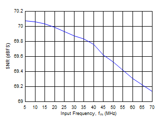
ADS52J90 D013_sbas623.gif
fSAMP = 80 MSPS
Figure 13. Signal-to-Noise Ratio vs fIN in
12-Bit, 16-Input Mode
ADS52J90 D015_sbas623.gif
fSAMP = 65 MSPS
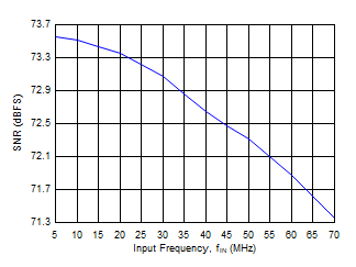
Figure 15. Signal-to-Noise Ratio vs fIN in
14-Bit, 16-Input Mode
ADS52J90 D017_sbas623.gif
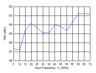
100-MSPS conversion clock
Figure 17. Second-Order Harmonic Distortion vs fIN
ADS52J90 D019_sbas623.gif
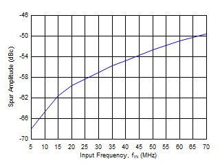
fSAMP = 200 MSPS
Figure 19. Input-Clock Intermodulation Spur at (fS / 2 ± fIN) vs fIN in 8-Input Mode
ADS52J90 D021_sbas623.gif
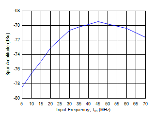
fSAMP = 200 MSPS
Figure 21. Input-Clock Intermodulation Spur at (fS / 4 ± fIN) vs fIN in 8-Input Mode
ADS52J90 D023_sbas623.gif
32-input mode, 14-bit resolution, fSAMP = 32.5 MSPS
Figure 23. Spurious-Free Dynamic Range vs AIN
ADS52J90 D025_sbas623.gif
16-input mode, 14-bit resolution, fSAMP = 65 MSPS
Figure 25. Signal-to-Noise Ratio vs Amplitude of
Differential Sine-Wave Input Clock
ADS52J90 D027_sbas623.gif
32-input mode, 14-bit resolution, fSAMP = 32.5 MSPS, –1-dBFS tone applied on one channel and spur on neighboring channel measured as crosstalk
Figure 27. Crosstalk vs fIN
ADS52J90 D029_sbas623.gif
32-input mode, 14-bit resolution, fSAMP = 32.5 MSPS
Figure 29. Differential Nonlinearity
ADS52J90 D031_sbas623.gif
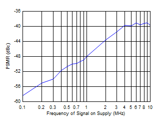
32-input mode; 14-bit resolution; fSAMP = 32.5 MSPS; 100-mVPP tone on supply; 5-MHz, –1-dBFS tone on input; PSMR is intermodulation tone referred to input tone amplitude
Figure 31. Power-Supply Modulation Ratio vs
Frequency of Signal on Supply
ADS52J90 D033_sbas623.gif
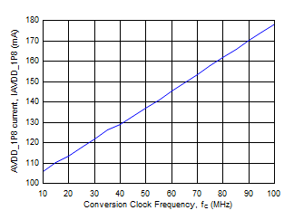
32-input mode, 10-bit resolution
Figure 33. AVDD_1P8 Current vs
Conversion Clock Frequency
ADS52J90 D035_sbas623.gif
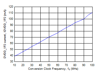
32-input mode, 10-bit resolution
Figure 35. DVDD_1P2 Current vs
Conversion Clock Frequency
ADS52J90 D044_sbas623.gif
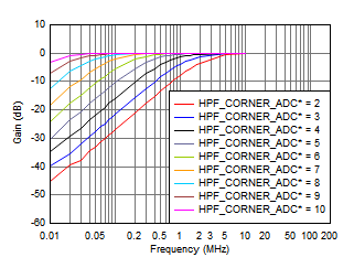
Figure 37. Digital High-Pass Filter Response
ADS52J90 D045_sbas623.gif
16-input mode, 12-bit resolution
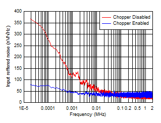
Figure 39. Low-Frequency Noise With and Without
Chopper Enabled