JAJSO07B December 2012 – April 2022 ADS54T01
PRODUCTION DATA
- 1 特長
- 2 アプリケーション
- 3 概要
- 4 Revision History
- 5 Device Comparison
- 6 Pin Configuration and Functions
- 7 Specifications
-
8 Detailed Description
- 8.1 Overview
- 8.2 Functional Block Diagram
- 8.3
Feature Description
- 8.3.1 Test Pattern Output
- 8.3.2 Clock Inputs
- 8.3.3 SNR and Clock Jitter
- 8.3.4 Analog Inputs
- 8.3.5 Over-Range Indication
- 8.3.6 Interleaving Correction
- 8.3.7 High-Resolution Output Data
- 8.3.8 Low-Resolution Output Data
- 8.3.9 Full Speed – 7 Bit
- 8.3.10 Decimated Low-Resolution Output Data
- 8.3.11 Multi Device Synchronization
- 8.4 Device Functional Modes
- 8.5 Programming
- 8.6 Register Maps
- 9 Power Supply Recommendations
- 10Device and Documentation Support
- 11Mechanical, Packaging, and Orderable Information
6 Pin Configuration and Functions
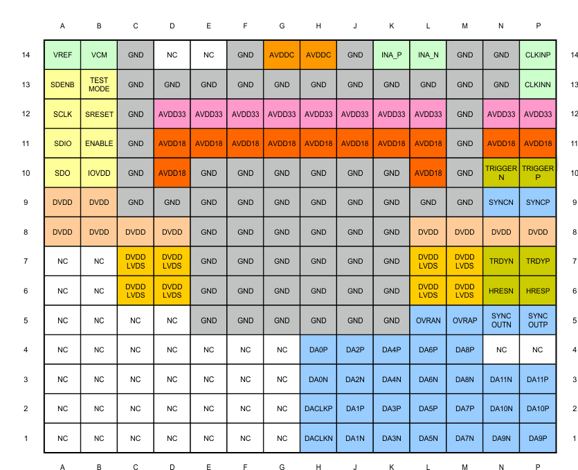
 Figure 6-1 ADS54T01 ZAY Package, 196-Pin NFBGA, Top View (DDR Output Mode)
Table 6-1 Pin Functions
| PIN | I/O TYPE(1) | DESCRIPTION | |
|---|---|---|---|
| NAME | NUMBER | ||
| INPUT/REFERENCE | |||
| INA_P/N | K14, L14 | I | Analog ADC differential input signal. |
| VCM | B14 | O | Output of the analog input common mode (nominally 1.9 V). A 0.1-μF capacitor to AGND is recommended, but not required. |
| VREF | A14 | I | Reference voltage input. A 0.1-μF capacitor to AGND is recommended. |
| CLOCK/SYNC | |||
| CLKINP/N | P14, P13 | I | Differential input clock |
| SYNCP/N | P9, N9 | I | Synchronization input. Inactive if logic low. When clocked in a high state initially, this is used for resetting internal clocks and digital logic and starting the SYNCOUT signal. Internal 100-Ω termination. |
| CONTROL/SERIAL | |||
| SRESET | B12 | I | Serial interface reset input. Active low. Initialized internal registers during high-to-low transition. Asynchronous. Internal 50-kΩ pullup resistor to IOVDD. |
| ENABLE | B11 | I | Chip enable – active high. Power-down function can be controlled through SPI register assignment. Internal 50-kΩ pullup resistor to IOVDD. |
| SCLK | A12 | I | Serial interface clock. Internal 50-kΩ pulldown resistor. |
| SDIO | A11 | I/O | Bidirectional serial data in 3-pin mode (default). In 4-pin interface mode (register x00, D16), the SDIO pin in an input only. Internal 50-kΩ pulldown resistor. |
| SDENB | A13 | I | Serial interface enable. Internal 50-kΩ pulldown resistor. |
| SDO | A10 | O | Uni-directional serial interface data in 4-pin mode (register x00, D16). The SDO pin is tri-stated in 3-pin interface mode (default). Internal 50-kΩ pulldown resistor. |
| DATA INTERFACE | |||
| DA[11:0]P/N | P3, N3, P2, N2, P1, N1, M4, M3, M2, M1, L4, L3, L2, L1, K4, K3, K2, K1, J4, J3, J2, J1, H4, H3 | O | ADC A Data Bits 11 (MSB) to 0 (LSB) in DDR output mode. Standard LVDS output. |
| DACLKP/N | H2, H1 | O | DDR differential output data clock for Bus A. Register programmable to provide either rising or falling edge to center of stable data nominal timing. |
| SYNCOUTP/N | P5, N5 | O | Synchronization output signal for synchronizing multiple ADCs. Can be disabled through the SPI. |
| OVRAP/N | M5, L5 | O | Bus A, Overrange indicator, LVDS output. A logic high signals an analog input in excess of the full-scale range. Optional SYNC output. |
| TRIGGERP/N | P10, N10 | I | Trigger used for high-resolution output data in feedback mode. Internal 100-Ω termination. |
| TRDYP/N | P7, N7 | O | Trigger ready output indicator |
| HRESP/N | P6, N6 | O | Indicator for high-resolution output data; logic high signals 12-bit output data. |
| NO CONNECT | |||
| NC | A1, A2, A3, A4, A5, A6, A7, B1, B2, B3, B4, B5, B6, B7, C1, C2, C3, C4, C5, D1, D2, D3, D4, D5, D14, E1, E2, E3, E4, E14, F1, F2, F3, F4, G1, G2, G3, G4, N4, P4 | – | Do not connect to pin, leave floating. |
| TESTMODE | B13 | – | Used for factory internal test. Do not connect to pin, leave floating. |
| POWER SUPPLY | |||
| AVDD33 | D12, E12, F12, G12, H12, J12, K12, L12, N12, P12 | P | 3.3-V analog supply |
| AVDDC | G14, H14 | P | 1.8-V supply for clock input |
| AVDD18 | D10, D11, E11, F11, G11, H11, J11, K11, L10, L11, N11, P11 | P | 1.8-V analog supply |
| DVDD | A8, A9, B8, B9, C8, D8, L8, M8, N8, P8 | P | 1.8-V supply for digital block |
| DVDDLVDS | C6, C7, D6, D7, L6, L7, M6, M7 | P | 1.8-V supply for LVDS outputs |
| IOVDD | B10 | P | 1.8-V for digital I/Os |
| GND | C9, C10, C11, C12, C13, C14, D9, D13, E5, E6, E7, E8, E9, E10, E13, F5, F6, F7, F8, F9, F10, F13, F14, G5, G6, G7, G8, G9, G10,H5, H6, H7, H8, H9, H10, J5, J6, J7, J8, J9, J10, K5, K6, K7, K8, K9, K10, L9, M9, M10, M11, M12, M13, M14,N13, N14 | GND | Ground |
(1) The definitions below define the I/O type for each pin.
- I = Input
- O = Output
- I/O = Input / Output
- P = Power Supply
- G = Ground