JAJSEC1C November   2019  – July 2020 ADS8686S

PRODUCTION DATA  

  1. 特長
  2. アプリケーション
  3. 概要
  4. Revision History
  5. Pin Configuration and Functions
  6. Specifications
    1. 6.1  Absolute Maximum Ratings
    2. 6.2  ESD Ratings
    3. 6.3  Recommended Operating Conditions
    4. 6.4  Thermal Information
    5. 6.5  Electrical Characteristics
    6. 6.6  Timing Requirements
    7. 6.7  Switching Characteristics
    8. 6.8  Timing Diagrams: Universal
    9. 6.9  Timing Diagrams: Parallel Data Read
    10. 6.10 Timing Diagrams: Serial Data Read
    11. 6.11 Typical Characteristics
  7. Detailed Description
    1. 7.1 Overview
    2. 7.2 Functional Block Diagram
    3. 7.3 Feature Description
      1. 7.3.1  Analog Inputs
      2. 7.3.2  Analog Input Impedance
      3. 7.3.3  Input Clamp Protection Circuit
      4. 7.3.4  Programmable Gain Amplifier (PGA)
      5. 7.3.5  Second-Order, Programmable, Low-Pass Filter (LPF)
      6. 7.3.6  ADC Driver
      7. 7.3.7  Multiplexer
      8. 7.3.8  Digital Filter and Noise
      9. 7.3.9  Reference
        1. 7.3.9.1 Internal Reference
        2. 7.3.9.2 External Reference
        3. 7.3.9.3 Supplying One VREF to Multiple Devices
      10. 7.3.10 ADC Transfer Function
    4. 7.4 Device Functional Modes
      1. 7.4.1 Device Interface: Pin Description
        1. 7.4.1.1  REFSEL (Input)
        2. 7.4.1.2  RESET (Input)
        3. 7.4.1.3  SEQEN (Input)
        4. 7.4.1.4  HW_RANGESEL[1:0] (Input)
        5. 7.4.1.5  SER/BYTE/PAR (Input)
        6. 7.4.1.6  DB[3:0] (Input/Output)
        7. 7.4.1.7  DB4/SER1W (Input/Output)
        8. 7.4.1.8  DB5/CRCEN (Input/Output)
        9. 7.4.1.9  DB[7:6] (Input/Output)
        10. 7.4.1.10 DB8 (Input/Output)
        11. 7.4.1.11 DB9/BYTESEL (Input/Output)
        12. 7.4.1.12 DB10/SDI (Input/Output)
        13. 7.4.1.13 DB11/SDOB (Input/Output)
        14. 7.4.1.14 DB12/SDOA (Input/Output)
        15. 7.4.1.15 DB13/OS0 (Input/Output)
        16. 7.4.1.16 DB14/OS1 (Input/Output)
        17. 7.4.1.17 DB15/OS2 (Input/Output)
        18. 7.4.1.18 WR/BURST (Input)
        19. 7.4.1.19 SCLK/RD (Input)
        20. 7.4.1.20 CS (Input)
        21. 7.4.1.21 CHSEL[2:0] (Input)
        22. 7.4.1.22 BUSY (Output)
        23. 7.4.1.23 CONVST (Input)
      2. 7.4.2 Device Modes of Operation
        1. 7.4.2.1 Shutdown Mode
        2. 7.4.2.2 Operation Mode
          1. 7.4.2.2.1 Hardware Mode
          2. 7.4.2.2.2 Software Mode
        3. 7.4.2.3 Reset Functionality
        4. 7.4.2.4 Channel Selection
          1. 7.4.2.4.1 Hardware Mode Channel Selection
          2. 7.4.2.4.2 Software Mode Channel Selection
        5. 7.4.2.5 Sequencer
          1. 7.4.2.5.1 Hardware Mode Sequencer
          2. 7.4.2.5.2 Software Mode Sequencer
        6. 7.4.2.6 Burst Sequencer
          1. 7.4.2.6.1 Hardware Mode Burst Sequencer
          2. 7.4.2.6.2 Software Mode Burst Sequencer
        7. 7.4.2.7 Diagnostics
          1. 7.4.2.7.1 Analog Diagnosis
          2. 7.4.2.7.2 Interface Diagnosis: SELF TEST and CRC
    5. 7.5 Programming
      1. 7.5.1 Parallel Interface
        1. 7.5.1.1 Reading Conversion Results
        2. 7.5.1.2 Writing Register Data
        3. 7.5.1.3 Reading Register Data
      2. 7.5.2 Parallel Byte Interface
        1. 7.5.2.1 Reading Conversion Results
        2. 7.5.2.2 Writing Register Data
        3. 7.5.2.3 Reading Register Data
      3. 7.5.3 Serial Interface
        1. 7.5.3.1 Reading Conversion Results
        2. 7.5.3.2 Writing Register Data
        3. 7.5.3.3 Reading Register Data
    6. 7.6 Register Maps
      1. 7.6.1 Page1 Registers
  8. Application and Implementation
    1. 8.1 Application Information
    2. 8.2 Typical Applications
      1. 8.2.1 8x2 Channel Data Acquisition System (DAQ) for Power Automation
        1. 8.2.1.1 Design Requirements
        2. 8.2.1.2 Detailed Design Procedure
        3. 8.2.1.3 Application Curve
      2. 8.2.2 Input Protection for Electrical Overstress
  9. Power Supply Recommendations
    1. 9.1 Power Supplies
  10. 10Layout
    1. 10.1 Layout Guidelines
    2. 10.2 Layout Examples
  11. 11Device and Documentation Support
    1. 11.1 Device Support
      1. 11.1.1 Development Support
    2. 11.2 Documentation Support
      1. 11.2.1 Related Documentation
    3. 11.3 Receiving Notification of Documentation Updates
    4. 11.4 サポート・リソース
    5. 11.5 Trademarks
    6. 11.6 Electrostatic Discharge Caution
    7. 11.7 Glossary

パッケージ・オプション

メカニカル・データ(パッケージ|ピン)
サーマルパッド・メカニカル・データ
発注情報

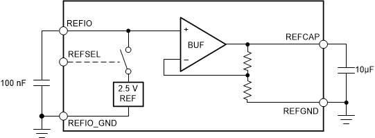
Internal Reference

The device has an internal 2.5-V (nominal value) band-gap reference. In order to select the internal reference, the REFSEL pin must be tied high or connected to DVDD. When the internal reference is used, REFIO (pin 33) becomes an output pin with the internal reference value. A 100-nF (minimum) decoupling capacitor, as illustrated in Figure 7-6, is recommended to be placed between the REFIO pin and REFIO_GND (pin 34). The capacitor must be placed as close to the REFIO pin as possible. The output impedance of the internal band-gap creates a low-pass filter with this capacitor to band-limit the noise of the band-gap output. Using a smaller capacitor increases the reference noise in the system, thus degrading SNR and SINAD performance. Do not use the REFIO pin to drive external AC or DC loads because of the limited current output capability of the pin. The REFIO pin can be used as a reference source if followed by a suitable op amp buffer.
GUID-E8A43400-D8C5-453E-89DA-FF6FAD478B91-low.gifFigure 7-6 Reference Circuitry