JAJSEC1C November 2019 – July 2020 ADS8686S
PRODUCTION DATA
- 1 特長
- 2 アプリケーション
- 3 概要
- 4 Revision History
- 5 Pin Configuration and Functions
-
6 Specifications
- 6.1 Absolute Maximum Ratings
- 6.2 ESD Ratings
- 6.3 Recommended Operating Conditions
- 6.4 Thermal Information
- 6.5 Electrical Characteristics
- 6.6 Timing Requirements
- 6.7 Switching Characteristics
- 6.8 Timing Diagrams: Universal
- 6.9 Timing Diagrams: Parallel Data Read
- 6.10 Timing Diagrams: Serial Data Read
- 6.11 Typical Characteristics
-
7 Detailed Description
- 7.1 Overview
- 7.2 Functional Block Diagram
- 7.3 Feature Description
- 7.4
Device Functional Modes
- 7.4.1
Device Interface: Pin Description
- 7.4.1.1 REFSEL (Input)
- 7.4.1.2 RESET (Input)
- 7.4.1.3 SEQEN (Input)
- 7.4.1.4 HW_RANGESEL[1:0] (Input)
- 7.4.1.5 SER/BYTE/PAR (Input)
- 7.4.1.6 DB[3:0] (Input/Output)
- 7.4.1.7 DB4/SER1W (Input/Output)
- 7.4.1.8 DB5/CRCEN (Input/Output)
- 7.4.1.9 DB[7:6] (Input/Output)
- 7.4.1.10 DB8 (Input/Output)
- 7.4.1.11 DB9/BYTESEL (Input/Output)
- 7.4.1.12 DB10/SDI (Input/Output)
- 7.4.1.13 DB11/SDOB (Input/Output)
- 7.4.1.14 DB12/SDOA (Input/Output)
- 7.4.1.15 DB13/OS0 (Input/Output)
- 7.4.1.16 DB14/OS1 (Input/Output)
- 7.4.1.17 DB15/OS2 (Input/Output)
- 7.4.1.18 WR/BURST (Input)
- 7.4.1.19 SCLK/RD (Input)
- 7.4.1.20 CS (Input)
- 7.4.1.21 CHSEL[2:0] (Input)
- 7.4.1.22 BUSY (Output)
- 7.4.1.23 CONVST (Input)
- 7.4.2 Device Modes of Operation
- 7.4.1
Device Interface: Pin Description
- 7.5 Programming
- 7.6 Register Maps
- 8 Application and Implementation
- 9 Power Supply Recommendations
- 10Layout
- 11Device and Documentation Support
7.5.3.1 Reading Conversion Results
A channel conversion is initiated when the CONVST signal transitions from low to high. The BUSY signal goes high and stays high to indicate an ongoing conversion. A data read cycle can be initiated after the BUSY signal goes low, indicating that the conversion is complete.
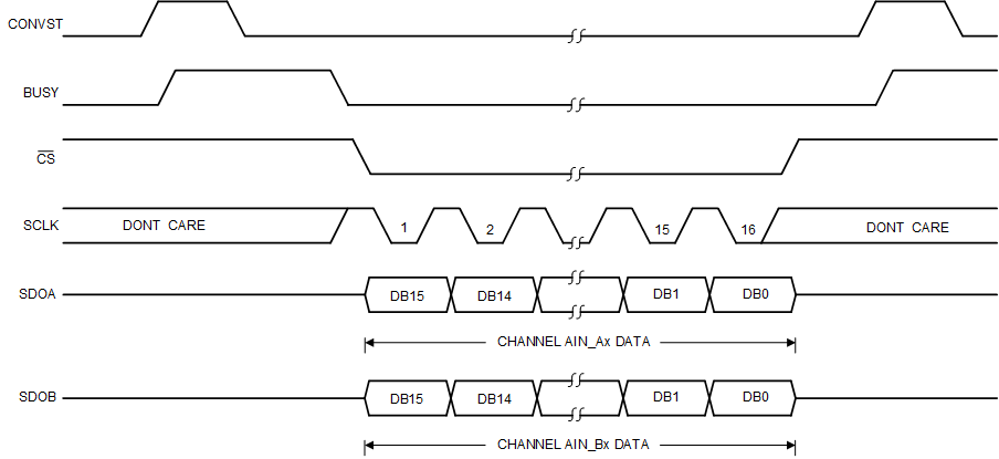
The CS falling edge takes the data output lines, SDOA and SDOB, out of tri-state and clocks out the MSB of the conversion result. The rising edge of SCLK clocks all subsequent data bits onto the serial data outputs, SDOA and SDOB. Figure 7-29 illustrates a read of two simultaneous conversion results using two SDOx lines on the ADS8686S. If the status register is appended to the conversion results or operates in sequencer burst mode where multiples of 16 SCLK transfers access data from the ADS8686S, hold CS low for the entire data frame. Data can also be clocked out using just the SDOA line. For the ADS8686S to access both the channel AIN_xA and channel AIN_xB conversion results on the SDOA line, a total of 32 SCLK cycles is required. Frame these 32 SCLK cycles using one CS signal, or individually frame each group of 16 SCLK cycles using the CS signal. The disadvantage of using just serial 1-wire mode is that the throughput rate is reduced.
Leave the unused SDOB line unconnected in serial 1-wire mode. If using SDOA as a single serial data output line, the channel results are output in the following order: AIN_xA and AIN_xB. Figure 7-30 shows a 1-wire, serial readback operation.
The speed at which the data can be read back in serial interface mode is dependent on the SPI frequency, DVDD supply, and the capacitance of the load on the SDO line, CLOAD. Table 7-10 shows a summary of the maximum speed achievable for various conditions.
| DVDD (V) | CLOAD (pF) | SPI FREQUENCY (MHz) |
|---|---|---|
| 1.8 to 3 | 20 | 40 |
| 3 to 5 | 30 | 50 |
 Figure 7-29 Serial Interface, 2-Wire Mode
 Figure 7-30 Serial Interface, 1-Wire Mode