JAJSHJ6B December 2011 – June 2019 AFE030
PRODUCTION DATA.
- 1 特長
- 2 アプリケーション
- 3 概要
- 4 改訂履歴
- 5 概要 (続き)
- 6 Pin Configuration and Functions
-
7 Specifications
- 7.1 Absolute Maximum Ratings
- 7.2 ESD Ratings
- 7.3 Thermal Information
- 7.4 Electrical Characteristics: Transmitter (Tx), Tx_DAC
- 7.5 Electrical Characteristics: Transmitter (Tx), Tx_PGA
- 7.6 Electrical Characteristics: Transmitter (Tx), Tx_FILTER
- 7.7 Electrical Characteristics: Power Amplifier (PA)
- 7.8 Electrical Characteristics: Receiver (Rx), Rx PGA1
- 7.9 Electrical Characteristics: Receiver (Rx), Rx Filter
- 7.10 Electrical Characteristics: Receiver (Rx), Rx PGA2
- 7.11 Electrical Characteristics: Digital
- 7.12 Electrical Characteristics: Two-Wire Interface
- 7.13 Electrical Characteristics: Zero-Crossing Detector
- 7.14 Electrical Characteristics: Internal Bias Generator
- 7.15 Electrical Characteristics: Power Supply
- 7.16 Typical Characteristics
- 8 Parameter Measurement Information
- 9 Detailed Description
- 10Application and Implementation
- 11デバイスおよびドキュメントのサポート
9.3.6 Zero Crossing Detector Block
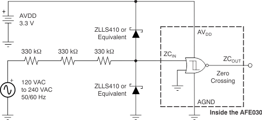
The AFE030 includes two zero crossing detectors. Zero crossing detectors can be used to synchronize communications signals to the ac line or sources of noise. Typically, in single-phase applications, only a single zero crossing detector is used. In three-phase applications, both zero crossing detectors can be used; one component detects phase A, and one detects phase B. Phase C zero crossings can then be inferred from the data gathered from the other phases. Figure 38 shows the AFE030 configured for non-isolated zero crossing detection.
 Figure 38. Non-Isolated Zero Crossing Detection Using the AFE030
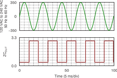
 Non-isolated zero crossing waveforms are shown in Figure 39.
 Figure 39. Non-Isolated Zero Crossing Waveforms
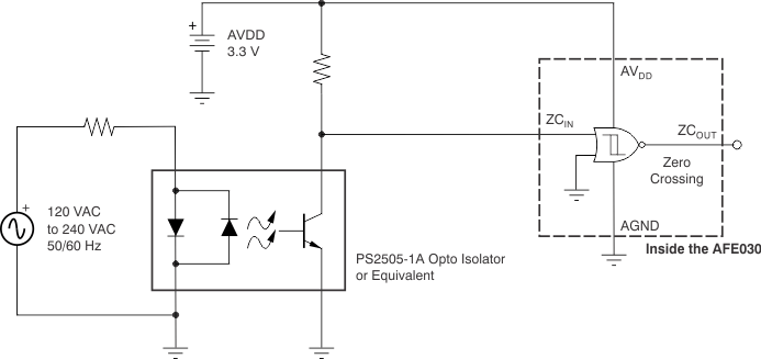
 For maximum protection of the AFE030 against line transients, it is recommended to use Schottky diodes as indicated in Figure 38. These diodes should limit the ZC_IN pins (pins 38 and 39) to within the maximum rating of (AVDD + 0.4 V) and (AGND – 0.4 V). Some applications may require an isolated zero crossing detection circuit. With a minimal amount of components, the AFE030 can be configured for isolated zero crossing detection, as Figure 40 shows.
 Figure 40. Isolated Zero Crossing Detection Using the AFE030
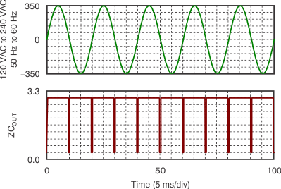
 Isolated zero crossing waveforms are shown in Figure 41.
 Figure 41. Isolated Zero Crossing Waveforms