JAJSQU7A July 2023 – February 2024 AWRL1432
ADVANCE INFORMATION
- 1
- 1 特長
- 2 アプリケーション
- 3 概要
- 4 機能ブロック図
- 5 Device Comparison
- 6 Terminal Configurations and Functions
-
7 Specifications
- 7.1 Absolute Maximum Ratings
- 7.2 ESD Ratings
- 7.3 Power-On Hours (POH)
- 7.4 Recommended Operating Conditions
- 7.5 Power Supply Specifications
- 7.6 Power Save Modes
- 7.7 Peak Current Requirement per Voltage Rail
- 7.8 RF Specification
- 7.9 Supported DFE Features
- 7.10 CPU Specifications
- 7.11 Thermal Resistance Characteristics
- 7.12
Timing and Switching Characteristics
- 7.12.1 Power Supply Sequencing and Reset Timing
- 7.12.2 Synchronized Frame Triggering
- 7.12.3 Input Clocks and Oscillators
- 7.12.4 MultiChannel buffered / Standard Serial Peripheral Interface (McSPI)
- 7.12.5 RDIF Interface Configuration
- 7.12.6 LIN
- 7.12.7 General-Purpose Input/Output
- 7.12.8 Controller Area Network - Flexible Data-rate (CAN-FD)
- 7.12.9 Serial Communication Interface (SCI)
- 7.12.10 Inter-Integrated Circuit Interface (I2C)
- 7.12.11 Quad Serial Peripheral Interface (QSPI)
- 7.12.12 JTAG Interface
-
8 Detailed Description
- 8.1 Overview
- 8.2 機能ブロック図
- 8.3 Subsystems
- 8.4 Other Subsystems
- 8.5 Memory Partitioning Options
- 8.6 Boot Modes
- 9 Applications, Implementation, and Layout
- 10Device and Documentation Support
- 11Revision History
- 12Mechanical, Packaging, and Orderable Information
7.12.3.1 Clock Specifications
The AWRL1432 requires external clock source (that is, a 40-MHz crystal or external oscillator to CLKP) for initial boot and as a reference for an internal APLL hosted in the device. An external crystal connected to the device pins Figure 7-8 shows the crystal implementation.
 Figure 7-8 Crystal Implementation
The load capacitors, Cf1 and Cf2 in Figure 7-8, should be chosen such that Equation 1 is satisfied. CL in the equation is the load specified by the crystal manufacturer. All discrete components used to implement the oscillator circuit should be placed as close as possible to the associated oscillator CLKP and CLKM pins.
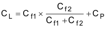
Table 7-13 lists the electrical characteristics of the clock crystal.
| NAME | DESCRIPTION | MIN | TYP | MAX | UNIT |
|---|---|---|---|---|---|
| fP | Parallel resonance crystal frequency | 40 | MHz | ||
| CL | Crystal load capacitance | 5 | 8 | 12 | pF |
| ESR | Crystal ESR | 50 | Ω | ||
| Temperature range | Expected temperature range of operation | –40 | 125 | °C | |
| Frequency tolerance | Crystal frequency tolerance(1)(2)(3) | –200 | 200 | ppm | |
| Drive level | 50 | 200 | µW | ||
In the case where an external clock is used as the clock resource, the signal is fed to the CLKP pin only; CLKM is grounded. The phase noise requirement is very important when a 40-MHz clock is fed externally. Table 7-14 lists the electrical characteristics of the external clock signal.
| PARAMETER | SPECIFICATION | UNIT | |||
|---|---|---|---|---|---|
| MIN | TYP | MAX | |||
| Input Clock: External AC-coupled sine wave or DC-coupled square wave Phase Noise referred to 40 MHz | Frequency | 40 | MHz | ||
| AC-Amplitude | 700 | 1200 | mV (pp) | ||
| DC-Vil | 0.00 | 0.20 | ns | ||
| DC-Vih | 1.6 | 1.95 | ns | ||
| Phase Noise at 1 kHz | –132 | dBc/Hz | |||
| Phase Noise at 10 kHz | –143 | dBc/Hz | |||
| Phase Noise at 100 kHz | –152 | dBc/Hz | |||
| Phase Noise at 1 MHz | –153 | dBc/Hz | |||
| Duty Cycle | 35 | 65 | % | ||
| Frequency Tolerance | -100 | 100 | ppm | ||