SLUSB76B February 2013 – May 2015
PRODUCTION DATA.
- 1 Features
- 2 Applications
- 3 Description
- 4 Revision History
- 5 Description (continued)
- 6 Pin Configuration and Functions
- 7 Specifications
-
8 Detailed Description
- 8.1 Overview
- 8.2 Functional Block Diagrams
- 8.3
Feature Description
- 8.3.1 Input Voltage Protection
- 8.3.2 Battery Protection
- 8.3.3 DEFAULT Mode
- 8.3.4 USB Friendly Power Up
- 8.3.5 Input Current Limiting at Power Up
- 8.3.6 Factory Mode
- 8.3.7 Spread Spectrum Mode
- 8.3.8 PWM Controller in Charge Mode
- 8.3.9 Battery Charging Process
- 8.3.10 Thermal Regulation and Protection
- 8.3.11 Charge Status Output, STAT Pin
- 8.3.12 Control Bits in Charge Mode
- 8.3.13 Control Pins in Charge Mode
- 8.3.14 Boost Mode Operation
- 8.3.15 High Impedance (Hi-Z) Mode
- 8.3.16 Serial Interface Description
- 8.4 Device Functional Modes
- 8.5 Register Maps
- 9 Application and Implementation
- 10Power Supply Recommendations
- 11Layout
- 12Device and Documentation Support
- 13Mechanical, Packaging, and Orderable Information
9 Application and Implementation
NOTE
Information in the following applications sections is not part of the TI component specification, and TI does not warrant its accuracy or completeness. TI’s customers are responsible for determining suitability of components for their purposes. Customers should validate and test their design implementation to confirm system functionality.
9.1 Application Information
The bq24157S is a compact, flexible, high-efficiency, USB-friendly, switch-mode charge management solution for single-cell Li-ion and Li-polymer batteries used in a wide range of portable applications. The bq24157S integrates a synchronous PWM controller, power MOSFETs, input current sensing, high-accuracy current and voltage regulation, and charge termination, into a small DSBGA package. The charge parameters can be programmed through an I2C interface.
9.2 Typical Application
VBUS = 5 V, ICHARGE = 1250 mA, VBAT = 3.5 to 4.44 V (adjustable).
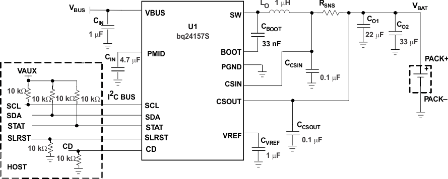 Figure 28. I2C Controlled 1-Cell USB Charger Application Circuit With USB-OTG Support
9.2.1 Design Requirements
Use the following typical application design procedure to select external components values for the bq24157S device.
| Specification | Test Condition | MIN | TYP | MAX | UNIT |
|---|---|---|---|---|---|
| Input DC voltage, VIN | Input voltage from AC adapter input | 4 | 5 | 6 | V |
| Input current | Maximum input current from AC adapter input | 0.1 | 0.1 to 0.5 | 1.5 | A |
| Charge current | Battery charge current | 0.325 | 0.7 | 1.55 | A |
| Output regulation voltage | Voltage applied at VBAT | 0 | 3 to 4.2 | 4.44 | V |
| Operating junction temperature range, TJ | 0 | 125 | °C | ||
9.2.2 Detailed Design Procedure
Systems design specifications:
- VBUS = 5 V
- VBAT = 4.2 V (1 cell)
- I(charge) = 1.25 A
- Inductor ripple current = 30% of fast charge current
- Determine the inductor value (LOUT) for the specified charge current ripple:
- Determine the output capacitor value (COUT) using 40 kHz as the resonant frequency:
- Determine the sense resistor using Equation 9:
- Measured efficiency and total power loss with different inductors are shown in Figure 29. SW node and inductor current waveform are shown in Figure 37.
 , the worst case is when battery voltage is as close as to half of the input voltage.

LOUT = 1.11 μH
Select the output inductor to standard 1 μH. Calculate the total ripple current with using the 1-μH inductor:


ΔIL = 0.42 A
Calculate the maximum output current:


ILPK = 1.46 A
Select 2.5-mm by 2-mm, 1-μH, 1.5-A surface mount multi-layer inductor. The suggested inductor part numbers are shown in Table 11.
Table 11. Inductor Part Numbers
| Part Number | Inductance | Size | Manufacturer |
|---|---|---|---|
| LQM2HPN1R0MJ0 | 1 μH | 2.5 × 2.0 mm | Murata |
| MIPS2520D1R0 | 1 μH | 2.5 × 2.0 mm | FDK |
| MDT2520-CN1R0M | 1 μH | 2.5 × 2.0 mm | TOKO |
| CP1008 | 1 μH | 2.5 × 2.0 mm | Inter-Technical |


COUT = 15.8 μF
Select two 0603 X5R 6.3-V 10-μF ceramic capacitors in parallel, that is, Murata GRM188R60J106M.

The maximum sense voltage across the sense resistor is 85 mV. To get a better current regulation accuracy, V(RSNS) should equal 85 mV, and calculate the value for the sense resistor.

R(SNS) = 68 mΩ
This is a standard value. If it is not a standard value, then choose the next close value and calculate the real charge current. Calculate the power dissipation on the sense resistor:
P(RSNS) = I(CHARGE)2 × R(SNS)
P(RSNS) = 1.252 × 0.068
P(RSNS) = 0.106 W
Select 0402 0.125-W 68-mΩ 2% sense resistor, that is, Panasonic ERJ2BWGR068.
For 1.5A application, R(SNS)= 85mV/1.55A = 55 mΩ
 Figure 29. Measured Efficiency and Power Loss
9.2.2.1 Charge Current Sensing Resistor Selection Guidelines
Both the termination current range and charge current range depend on the sensing resistor (RSNS). The termination current step (IOTERM_STEP) can be calculated using Equation 11.

Table 12 shows the termination current settings for three sensing resistors.
Table 12. Termination Current Settings for 55-mΩ, 68-mΩ, and 100-mΩ Sense Resistors
| BIT | VI(TERM) (mV) | I(TERM) (mA) R(SNS) = 55 mΩ |
I(TERM) (mA) R(SNS) = 68 mΩ |
I(TERM) (mA) R(SNS) = 100 mΩ |
|---|---|---|---|---|
| VI(TERM2) | 13.6 | 247 | 200 | 136 |
| VI(TERM1) | 6.8 | 124 | 100 | 68 |
| VI(TERM0) | 3.4 | 62 | 50 | 34 |
| Offset | 3.4 | 62 | 50 | 34 |
For example, with a 68-mΩ sense resistor, V(ITERM2) = 1, V(ITERM1) = 0, and V(ITERM0) = 1, ITERM = [(13.6 mV × 1) + (6.8 mV × 0) + (3.4 mV × 1) + 3.4 mV] / 68 mΩ = 200 mA + 0 + 50 mA + 50 mA = 300 mA.
The charge current step (IO(CHARGE_STEP)) is calculated using Equation 12.

Table 13 shows the charge current settings for three sensing resistors.
Table 13. Charge Current Settings for 55-mΩ, 68-mΩ, and 100-mΩ Sense Resistors
| BIT | VI(REG) (mV) | IO(CHARGE) (mA) R(SNS) = 55 mΩ |
IO(CHARGE) (mA) R(SNS) = 68 mΩ |
IO(CHARGE) (mA) R(SNS) = 100 mΩ |
|---|---|---|---|---|
| VI(CHRG3) | 54.4 | 989 | 800 | 544 |
| VI(CHRG2) | 27.2 | 495 | 400 | 272 |
| VI(CHRG1) | 13.6 | 247 | 200 | 136 |
| VI(CHRG0) | 6.8 | 124 | 100 | 68 |
| Offset | 37.4 | 680 | 550 | 374 |
For example, with a 68-mΩ sense resistor, V(CHRG3) = 1, V(CHRG2) = 0, V(ICHRG1) = 0, and V(ICHRG0) = 1, ITERM = [(54.4 mV × 1) + (27.2 mV × 0) + (13.6 mV × 0) + (6.8 mV × 1) + 37.4 mV] / 68 mΩ = 800 mA + 0 + 0 + 100 mA = 900 mA.
9.2.2.2 Output Inductor and Capacitance Selection Guidelines
The IC provides internal loop compensation. With the internal loop compensation, the highest stability occurs when the LC resonant frequency, ƒo, is approximately 40 kHz (20 to 80 kHz). Equation 13 can be used to calculate the value of the output inductor, LOUT, and output capacitor, COUT.

To reduce the output voltage ripple, TI recommends a ceramic capacitor with the capacitance between 4.7 to 47 μF for COUT. See previous sections in the Detailed Design Procedure for components selection.
9.2.3 Application Curves
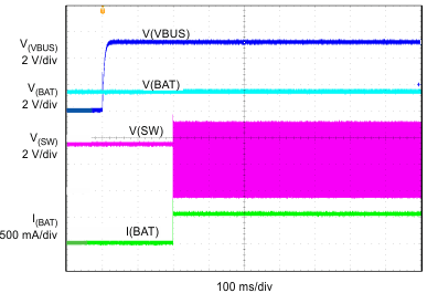
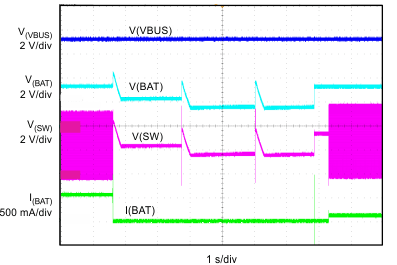
| VBUS = 0 to 5 V | IIN_limit = 500 mA | VBATREG = 4.2 V |
| VBAT = 3.5 V | ICHG = 550 mA | |
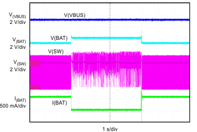
| VBUS = 5 V | VBAT = 3.5 V | IIN_limit = 500 mA |
| VBATREG = 4.2 V | ICHG = 550 mA | Termination Enabled |
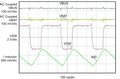
| VBUS = 5.05 V | VBAT = 3.5 V | IBUS = 217 mA |
| VBUS = 5 V | VBAT = 3.5 V | IIN_limit = 500 mA |
| VBATREG = 4.2 V | ICHG = 550 mA | |
| Termination Enabled | ||
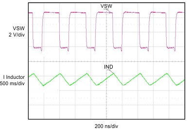
| VBUS = 5 V | VBAT = 2.6 V | VOREG = 4.2 V |
| ICHG = 950 mA |
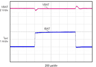
| 5.5-V input voltage |