SLUSB76B February   2013  – May 2015

PRODUCTION DATA.  

  1. Features
  2. Applications
  3. Description
  4. Revision History
  5. Description (continued)
  6. Pin Configuration and Functions
  7. Specifications
    1. 7.1 Absolute Maximum Ratings
    2. 7.2 ESD Ratings
    3. 7.3 Recommended Operating Conditions
    4. 7.4 Thermal Information
    5. 7.5 Electrical Characteristics
    6. 7.6 Typical Performance Characteristics
  8. Detailed Description
    1. 8.1 Overview
    2. 8.2 Functional Block Diagrams
    3. 8.3 Feature Description
      1. 8.3.1  Input Voltage Protection
        1. 8.3.1.1 Input Overvoltage Protection
        2. 8.3.1.2 Bad Adaptor Detection/Rejection
        3. 8.3.1.3 Sleep Mode
        4. 8.3.1.4 Input Voltage Based DPM (Special Charger Voltage Threshold)
      2. 8.3.2  Battery Protection
        1. 8.3.2.1 Output Overvoltage Protection
        2. 8.3.2.2 Battery Short Protection
        3. 8.3.2.3 Battery Detection in HOST Mode
      3. 8.3.3  DEFAULT Mode
      4. 8.3.4  USB Friendly Power Up
      5. 8.3.5  Input Current Limiting at Power Up
      6. 8.3.6  Factory Mode
      7. 8.3.7  Spread Spectrum Mode
      8. 8.3.8  PWM Controller in Charge Mode
      9. 8.3.9  Battery Charging Process
      10. 8.3.10 Thermal Regulation and Protection
      11. 8.3.11 Charge Status Output, STAT Pin
      12. 8.3.12 Control Bits in Charge Mode
        1. 8.3.12.1 CE Bit (Charge Mode)
        2. 8.3.12.2 RESET Bit
        3. 8.3.12.3 OPA_MODE Bit
      13. 8.3.13 Control Pins in Charge Mode
        1. 8.3.13.1 CD Pin (Charge Disable)
      14. 8.3.14 Boost Mode Operation
        1. 8.3.14.1 PWM Controller in Boost Mode
        2. 8.3.14.2 Boost Start Up
        3. 8.3.14.3 PFM Mode at Light Load
        4. 8.3.14.4 Protection in Boost Mode
          1. 8.3.14.4.1 Output Overvoltage Protection
          2. 8.3.14.4.2 Output Overload Protection
          3. 8.3.14.4.3 Battery Overvoltage Protection
        5. 8.3.14.5 STAT Pin in Boost Mode
      15. 8.3.15 High Impedance (Hi-Z) Mode
      16. 8.3.16 Serial Interface Description
        1. 8.3.16.1 F/S Mode Protocol
        2. 8.3.16.2 HS Mode Protocol
        3. 8.3.16.3 I2C Update Sequence
        4. 8.3.16.4 Slave Address Byte
        5. 8.3.16.5 Register Address Byte
    4. 8.4 Device Functional Modes
      1. 8.4.1 Charge Mode Operation
        1. 8.4.1.1 Charge Profile
    5. 8.5 Register Maps
  9. Application and Implementation
    1. 9.1 Application Information
    2. 9.2 Typical Application
      1. 9.2.1 Design Requirements
      2. 9.2.2 Detailed Design Procedure
        1. 9.2.2.1 Charge Current Sensing Resistor Selection Guidelines
        2. 9.2.2.2 Output Inductor and Capacitance Selection Guidelines
      3. 9.2.3 Application Curves
  10. 10Power Supply Recommendations
    1. 10.1 System Load After Sensing Resistor
  11. 11Layout
    1. 11.1 Layout Guidelines
    2. 11.2 Layout Example
  12. 12Device and Documentation Support
    1. 12.1 Device Support
      1. 12.1.1 Third-Party Products Disclaimer
    2. 12.2 Documentation Support
      1. 12.2.1 Related Documentation
    3. 12.3 Trademarks
    4. 12.4 Electrostatic Discharge Caution
    5. 12.5 Glossary
  13. 13Mechanical, Packaging, and Orderable Information
    1. 13.1 Package Summary
      1. 13.1.1 Chip Scale Packaging Dimensions

パッケージ・オプション

メカニカル・データ(パッケージ|ピン)
サーマルパッド・メカニカル・データ
発注情報

13 Mechanical, Packaging, and Orderable Information

The following pages include mechanical, packaging, and orderable information. This information is the most current data available for the designated devices. This data is subject to change without notice and revision of this document. For browser-based versions of this data sheet, refer to the left-hand navigation.

13.1 Package Summary
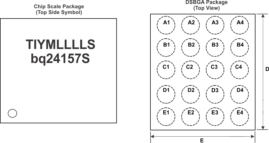
bq24157S package_summary_lusb76.gif
0-Pin A1 Marker , TI-TI Letters, YM = Year Month Date Code, LLLL = Lot T race Code, S = Assembly Site Code

13.1.1 Chip Scale Packaging Dimensions

The bq24157S device is available in a 20-bump chip scale package (DSBGA, NanoFree™).

The package dimensions are:

D E
Max = 2.17 mm Max = 2.03 mm
Min = 2.11 mm Min = 1.97 mm