SLUSBS8B December 2013 – November 2019 BQ40Z50
PRODUCTION DATA.
- 1 Features
- 2 Applications
- 3 Description
- 4 Revision History
- 5 Description (continued)
- 6 Pin Configuration and Functions
-
7 Specifications
- 7.1 Absolute Maximum Ratings
- 7.2 ESD Ratings
- 7.3 Recommended Operating Conditions
- 7.4 Thermal Information
- 7.5 Electrical Characteristics: Supply Current
- 7.6 Electrical Characteristics: Power Supply Control
- 7.7 Electrical Characteristics: AFE Power-On Reset
- 7.8 Electrical Characteristics: AFE Watchdog Reset and Wake Timer
- 7.9 Electrical Characteristics: Current Wake Comparator
- 7.10 Electrical Characteristics: VC1, VC2, VC3, VC4, BAT, PACK
- 7.11 Electrical Characteristics: SMBD, SMBC
- 7.12 Electrical Characteristics: PRES, BTP_INT, DISP
- 7.13 Electrical Characteristics: LEDCNTLA, LEDCNTLB, LEDCNTLC
- 7.14 Electrical Characteristics: Coulomb Counter
- 7.15 Electrical Characteristics: CC Digital Filter
- 7.16 Electrical Characteristics: ADC
- 7.17 Electrical Characteristics: ADC Digital Filter
- 7.18 Electrical Characteristics: CHG, DSG FET Drive
- 7.19 Electrical Characteristics: PCHG FET Drive
- 7.20 Electrical Characteristics: FUSE Drive
- 7.21 Electrical Characteristics: Internal Temperature Sensor
- 7.22 Electrical Characteristics: TS1, TS2, TS3, TS4
- 7.23 Electrical Characteristics: PTC, PTCEN
- 7.24 Electrical Characteristics: Internal 1.8-V LDO
- 7.25 Electrical Characteristics: High-Frequency Oscillator
- 7.26 Electrical Characteristics: Low-Frequency Oscillator
- 7.27 Electrical Characteristics: Voltage Reference 1
- 7.28 Electrical Characteristics: Voltage Reference 2
- 7.29 Electrical Characteristics: Instruction Flash
- 7.30 Electrical Characteristics: Data Flash
- 7.31 Electrical Characteristics: OCD, SCC, SCD1, SCD2 Current Protection Thresholds
- 7.32 Timing Requirements: OCD, SCC, SCD1, SCD2 Current Protection Timing
- 7.33 Timing Requirements: SMBus
- 7.34 Timing Requirements: SMBus XL
- 7.35 Typical Characteristics
-
8 Detailed Description
- 8.1 Overview
- 8.2 Functional Block Diagram
- 8.3
Feature Description
- 8.3.1 Primary (1st Level) Safety Features
- 8.3.2 Secondary (2nd Level) Safety Features
- 8.3.3 Charge Control Features
- 8.3.4 Gas Gauging
- 8.3.5 Configuration
- 8.3.6 Battery Parameter Measurements
- 8.3.7 Battery Trip Point (BTP)
- 8.3.8 Lifetime Data Logging Features
- 8.3.9 Authentication
- 8.3.10 LED Display
- 8.3.11 Voltage
- 8.3.12 Current
- 8.3.13 Temperature
- 8.3.14 Communications
- 8.4 Device Functional Modes
- 9 Applications and Implementation
- 10Power Supply Recommendations
- 11Layout
- 12Device and Documentation Support
- 13Mechanical, Packaging, and Orderable Information
パッケージ・オプション
メカニカル・データ(パッケージ|ピン)
- RSM|32
サーマルパッド・メカニカル・データ
- RSM|32
発注情報
9.2.2.1.2 Chemical Fuse
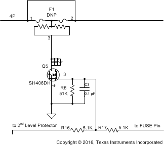
The chemical fuse (Dexerials, Uchihashi, and so forth) is ignited under command from either the bq294700 secondary voltage protection IC or from the FUSE pin of the gas gauge. Either of these events applies a positive voltage to the gate of Q5, shown in Figure 23, which then sinks current from the third terminal of the fuse, causing it to ignite and open permanently.
It is important to carefully review the fuse specifications and match the required ignition current to that available from the N-channel FET. Ensure that the proper voltage, current, and Rds(on) ratings are used for this device. The fuse control circuit is discussed in detail in FUSE Circuitry.
 Figure 23. FUSE Circuit