JAJSU42A April 2022 – April 2024 BQ76922
PRODUCTION DATA
- 1
- 1 特長
- 2 アプリケーション
- 3 概要
- 4 Device Comparison Table
- 5 Pin Configuration and Functions
-
6 Specifications
- 6.1 Absolute Maximum Ratings
- 6.2 ESD Ratings
- 6.3 Recommended Operating Conditions
- 6.4 Thermal Information BQ76922
- 6.5 Supply Current
- 6.6 Digital I/O
- 6.7 LD Pin
- 6.8 Precharge (PCHG) and Predischarge (PDSG) FET Drive
- 6.9 FUSE Pin Functionality
- 6.10 REG18 LDO
- 6.11 REG0 Pre-regulator
- 6.12 REG1 LDO
- 6.13 Voltage References
- 6.14 Coulomb Counter
- 6.15 Coulomb Counter Digital Filter (CC1)
- 6.16 Current Measurement Digital Filter (CC2)
- 6.17 Current Wake Detector
- 6.18 Analog-to-Digital Converter
- 6.19 Cell Balancing
- 6.20 Cell Open Wire Detector
- 6.21 Internal Temperature Sensor
- 6.22 Thermistor Measurement
- 6.23 Internal Oscillators
- 6.24 High-side NFET Drivers
- 6.25 Comparator-Based Protection Subsystem
- 6.26 Timing Requirements – I2C Interface, 100kHz Mode
- 6.27 Timing Requirements – I2C Interface, 400kHz Mode
- 6.28 Timing Requirements – HDQ Interface
- 6.29 Interface Timing Diagrams
- 6.30 Typical Characteristics
-
7 Detailed Description
- 7.1 Overview
- 7.2 Functional Block Diagram
- 7.3 Diagnostics
- 7.4 Device Configuration
- 7.5
Measurement Subsystem
- 7.5.1 Voltage Measurement
- 7.5.2 General Purpose ADCIN Functionality
- 7.5.3 Coulomb Counter and Digital Filters
- 7.5.4 Synchronized Voltage and Current Measurement
- 7.5.5 Internal Temperature Measurement
- 7.5.6 Thermistor Temperature Measurement
- 7.5.7 Factory Trim of Voltage ADC
- 7.5.8 Voltage Calibration (ADC Measurements)
- 7.5.9 Voltage Calibration (COV and CUV Protections)
- 7.5.10 Current Calibration
- 7.5.11 Temperature Calibration
- 7.6 Primary and Secondary Protection Subsystems
- 7.7
Device
Hardware Features
- 7.7.1 Voltage References
- 7.7.2 ADC Multiplexer
- 7.7.3 LDOs
- 7.7.4 Standalone Versus Host Interface
- 7.7.5 Multifunction Pin Controls
- 7.7.6 RST_SHUT Pin Operation
- 7.7.7 CFETOFF, DFETOFF, and BOTHOFF Pin Functionality
- 7.7.8 ALERT Pin Operation
- 7.7.9 Fuse Drive
- 7.7.10 Cell Open Wire
- 7.7.11 Low Frequency Oscillator
- 7.7.12 High Frequency Oscillator
- 7.8 Device Functional Modes
- 7.9 Serial Communications Interface
- 7.10 Cell Balancing
- 8 Application and Implementation
- 9 Power Supply Requirements
- 10Layout
- 11Device and Documentation Support
- 12Revision History
- 13Mechanical, Packaging, Orderable Information
パッケージ・オプション
デバイスごとのパッケージ図は、PDF版データシートをご参照ください。
メカニカル・データ(パッケージ|ピン)
- RSN|32
サーマルパッド・メカニカル・データ
発注情報
10.2 Layout Example
The BQ76922EVM (see BQ76922EVM User Guide) provides an example circuit implementation using the BQ76922. The EVM is a 3.0-inch × 4.9-inch 4-layer circuit card assembly and is designed for easy assembly, with cell connections at a terminal block on the left edge, and pack connections using a second terminal block on the top edge of the board. Wide trace areas are used, reducing voltage drops on the high current paths. Optional connections for hardware feature pins are on a separate terminal block on the top edge of the board. An on-board microcontroller is included for interfacing with a computer, with the accompanying USB connector located in the lower right corner. Configuration headers are included toward the right side of the board, and pushbutton switches for wake up and reset of the BQ76922 are located near the bottom edge of the board.
The board layout includes spark gaps with the reference designator prefix E. These spark gaps are fabricated with the board and no component is installed.
Figure 10-1 to Figure 10-8 show the board layout.
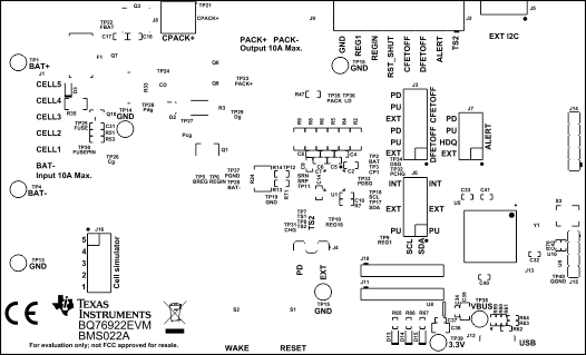 Figure 10-1 BQ76922EVM Top Silk Screen
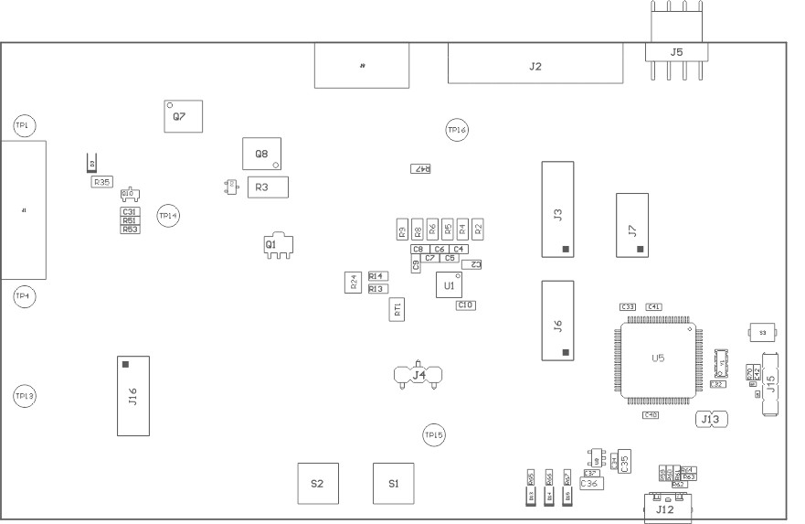 Figure 10-2 BQ76922EVM Top Assembly
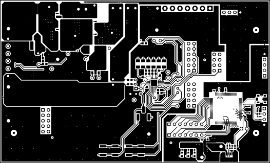 Figure 10-3 BQ76922EVM Top Layer
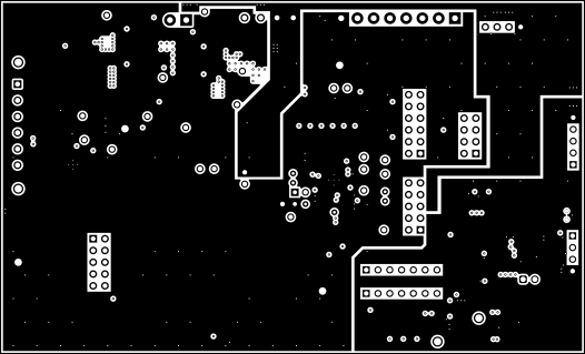 Figure 10-4 BQ76922EVM Layer 2
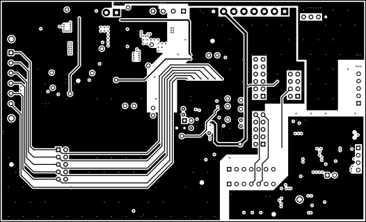 Figure 10-5 BQ76922EVM Layer 3
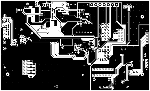 Figure 10-6 BQ76922EVM Bottom Layer
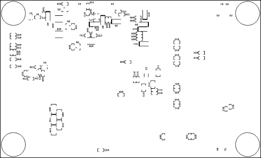 Figure 10-7 BQ76922EVM Bottom Silk Screen
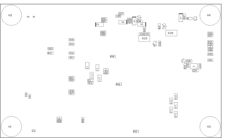 Figure 10-8 BQ76922EVM Bottom Assembly