JAJSDP2C April   2016  – February 2022 CSD17382F4

PRODUCTION DATA  

  1. 1特長
  2. 2アプリケーション
  3. 3概要
  4. 4Revision History
  5. 5Specifications
    1. 5.1 Electrical Characteristics
    2. 5.2 Thermal Information
    3. 5.3 Typical MOSFET Characteristics
  6. 6Device and Documentation Support
    1. 6.1 サポート・リソース
    2. 6.2 Receiving Notification of Documentation Updates
    3. 6.3 Trademarks
    4. 6.4 Electrostatic Discharge Caution
    5. 6.5 Glossary
  7. 7Mechanical, Packaging, and Orderable Information
    1. 7.1 Mechanical Dimensions
    2. 7.2 Recommended Minimum PCB Layout
    3. 7.3 Recommended Stencil Pattern
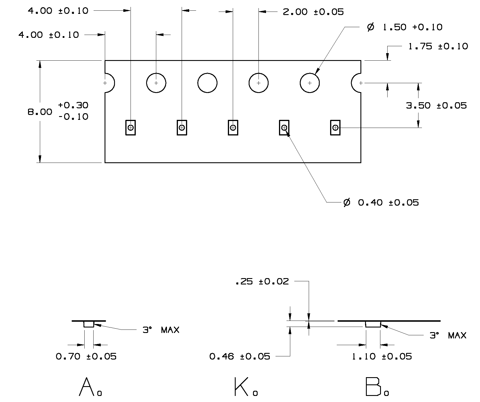
    4. 7.4 CSD17382F4 Embossed Carrier Tape Dimensions

パッケージ・オプション

デバイスごとのパッケージ図は、PDF版データシートをご参照ください。

メカニカル・データ(パッケージ|ピン)
  • YJC|3
サーマルパッド・メカニカル・データ
発注情報

CSD17382F4 Embossed Carrier Tape Dimensions

GUID-7F249C4A-1F3F-4C99-8D79-B1DAF1C6652D-low.png
Pin 1 is oriented in the top-right quadrant of the tape enclosure (quadrant 2), closest to the carrier tape sprocket holes.