JAJSFA3B September   2012  – April 2018 CSD86360Q5D

PRODUCTION DATA.  

  1. 1特長
  2. 2アプリケーション
  3. 3概要
    1. 3.1 上面図
      1.      Device Images
        1.       回路例
        2.       標準的なパワー・ブロックの効率と電力損失との関係
  4. 4改訂履歴
  5. 5Specifications
    1. 5.1 Absolute Maximum Ratings
    2. 5.2 Recommended Operating Conditions
    3. 5.3 Power Block Performance
    4. 5.4 Thermal Information
    5. 5.5 Electrical Characteristics
    6. 5.6 Typical Power Block Device Characteristics
    7. 5.7 Typical Power Block MOSFET Characteristics
  6. 6Application and Implementation
    1. 6.1 Application Information
      1. 6.1.1 Equivalent System Performance
      2. 6.1.2 Power Loss Curves
      3. 6.1.3 Safe Operating Area (SOA) Curves
      4. 6.1.4 Normalized Curves
    2. 6.2 Typical Application
      1. 6.2.1 Design Example: Calculating Power Loss and SOA
        1. 6.2.1.1 Operating Conditions
        2. 6.2.1.2 Calculating Power Loss
        3. 6.2.1.3 Calculating SOA Adjustments
  7. 7Layout
    1. 7.1 Layout Guidelines
      1. 7.1.1 Electrical Performance
      2. 7.1.2 Thermal Performance
    2. 7.2 Layout Example
  8. 8デバイスおよびドキュメントのサポート
    1. 8.1 ドキュメントのサポート
      1. 8.1.1 関連資料
    2. 8.2 ドキュメントの更新通知を受け取る方法
    3. 8.3 コミュニティ・リソース
    4. 8.4 商標
    5. 8.5 静電気放電に関する注意事項
    6. 8.6 Glossary
  9. 9メカニカル、パッケージ、および注文情報
    1. 9.1 Q5Dパッケージの寸法
    2. 9.2 推奨ランド・パターン
    3. 9.3 推奨ステンシル
    4. 9.4 Q5Dのテープ・アンド・リール情報

パッケージ・オプション

メカニカル・データ(パッケージ|ピン)
サーマルパッド・メカニカル・データ
発注情報

Calculating SOA Adjustments

  • SOA adjustment for input voltage ≈ 1.3°C (Figure 7)
  • SOA adjustment for output voltage ≈ –2.5°C (Figure 8)
  • SOA adjustment for switching frequency ≈ 6.0°C (Figure 6)
  • SOA adjustment for output inductor ≈ 1.3°C (Figure 9)
  • Final calculated SOA adjustment = 1.3 + (–2.5) + 6.0 + 1.3 ≈ 6.1°C

In the design example above, the estimated power loss of the CSD86360Q5D would increase to 3.84 W. In addition, the maximum allowable board and/or ambient temperature would have to decrease by 6.1°C. Figure 33 graphically shows how the SOA curve would be adjusted accordingly.

  1. Start by drawing a horizontal line from the application current to the SOA curve.
  2. Draw a vertical line from the SOA curve intercept down to the board/ambient temperature.
  3. Adjust the SOA board/ambient temperature by subtracting the temperature adjustment value.

In the design example, the SOA temperature adjustment yields a reduction in allowable board/ambient temperature of 6.1°C. In the event the adjustment value is a negative number, subtracting the negative number would yield an increase in allowable board/ambient temperature.
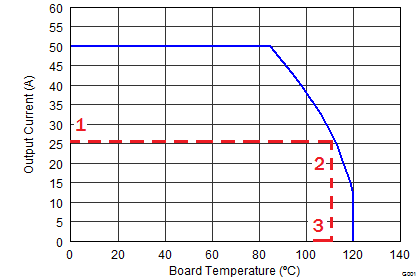
CSD86360Q5D soa_example.pngFigure 33. Power Block SOA