JAJSE15B February   2016  – April 2018 CSD87335Q3D

PRODUCTION DATA.  

  1. 1特長
  2. 2アプリケーション
  3. 3概要
    1.     上面図
      1.      Device Images
  4. 4改訂履歴
  5. 5Specifications
    1. 5.1 Absolute Maximum Ratings
    2. 5.2 Recommended Operating Conditions
    3. 5.3 Thermal Information
    4. 5.4 Power Block Performance
    5. 5.5 Electrical Characteristics
    6. 5.6 Typical Power Block Device Characteristics
    7. 5.7 Typical Power Block MOSFET Characteristics
  6. 6Applications and Implementation
    1. 6.1 Application Information
      1. 6.1.1 Equivalent System Performance
    2. 6.2 Power Loss Curves
    3. 6.3 Safe Operating Curves (SOA)
    4. 6.4 Normalized Curves
    5. 6.5 Calculating Power Loss and SOA
      1. 6.5.1 Design Example
      2. 6.5.2 Calculating Power Loss
      3. 6.5.3 Calculating SOA Adjustments
  7. 7Recommended PCB Design Overview
    1. 7.1 Electrical Performance
    2. 7.2 Thermal Performance
  8. 8デバイスおよびドキュメントのサポート
    1. 8.1 ドキュメントの更新通知を受け取る方法
    2. 8.2 コミュニティ・リソース
    3. 8.3 商標
    4. 8.4 静電気放電に関する注意事項
    5. 8.5 Glossary
  9. 9メカニカル、パッケージ、および注文情報
    1. 9.1 Q3Dパッケージの寸法
    2. 9.2 推奨ランド・パターン
    3. 9.3 推奨ステンシル
    4. 9.4 Q3Dのテープ・アンド・リール情報
    5. 9.5 ピン構成

パッケージ・オプション

メカニカル・データ(パッケージ|ピン)
サーマルパッド・メカニカル・データ
発注情報

Thermal Performance

The power block has the ability to utilize the GND planes as the primary thermal path. As such, the use of thermal vias is an effective way to pull away heat from the device and into the system board. Concerns of solder voids and manufacturability problems can be addressed by the use of three basic tactics to minimize the amount of solder attach that will wick down the via barrel:

  • Intentionally space out the vias from each other to avoid a cluster of holes in a given area.
  • Use the smallest drill size allowed in your design. The example in Figure 33 uses vias with a 10-mil drill hole and a 16-mil capture pad.
  • Tent the opposite side of the via with solder-mask.

In the end, the number and drill size of the thermal vias should align with the end user’s PCB design rules and manufacturing capabilities.
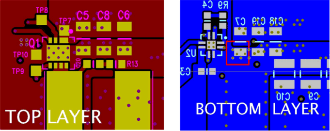
CSD87335Q3D RecPCBLayout.gifFigure 33. Recommended PCB Layout (Top Down)